SBASAW0 February 2024 ADS1288
PRODUCTION DATA
- 1
- 1 Features
- 2 Applications
- 3 Description
- 4 Pin Configuration and Functions
-
5 Specifications
- 5.1 Absolute Maximum Ratings
- 5.2 ESD Ratings
- 5.3 Recommended Operating Conditions
- 5.4 Thermal Information
- 5.5 Electrical Characteristics
- 5.6 Timing Requirements: 1.65V ≤ IOVDD ≤ 1.95V and 2.7V ≤ IOVDD ≤ 3.6V
- 5.7 Switching Characteristics: 1.65V ≤ IOVDD ≤ 1.95V and 2.7V ≤ IOVDD ≤ 3.6V
- 5.8 Timing Diagrams
- 5.9 Typical Characteristics
- 6 Parameter Measurement Information
-
7 Detailed Description
- 7.1 Overview
- 7.2 Functional Block Diagram
- 7.3 Feature Description
- 7.4 Device Functional Modes
- 7.5
Programming
- 7.5.1 Serial Interface
- 7.5.2 Conversion Data Format
- 7.5.3
Commands
- 7.5.3.1 Single Byte Command
- 7.5.3.2 WAKEUP: Wake Command
- 7.5.3.3 STANDBY: Software Power-Down Command
- 7.5.3.4 SYNC: Synchronize Command
- 7.5.3.5 RESET: Reset Command
- 7.5.3.6 Read Data Direct
- 7.5.3.7 RDATA: Read Conversion Data Command
- 7.5.3.8 RREG: Read Register Command
- 7.5.3.9 WREG: Write Register Command
- 7.5.3.10 OFSCAL: Offset Calibration Command
- 7.5.3.11 GANCAL: Gain Calibration Command
-
8 Register Map
- 8.1
Register Descriptions
- 8.1.1 ID/SYNC: Device ID, SYNC Register (Address = 00h) [Reset = xxxx0010b]
- 8.1.2 CONFIG0: Configuration Register 0 (Address = 01h) [Reset = 92h]
- 8.1.3 CONFIG1: Configuration Register 1 (Address = 02h) [Reset = 10h]
- 8.1.4 HPF0, HPF1: High-Pass Filter Registers (Address = 03h, 04h) [Reset = 32h, 03h]
- 8.1.5 OFFSET0, OFFSET1, OFFSET2: Offset Calibration Registers (Address = 05h, 06h, 07h) [Reset = 00h, 00h, 00h]
- 8.1.6 GAIN0, GAIN1, GAIN2: Gain Calibration Registers (Address = 08h, 09h, 0Ah) [Reset = 00h, 00h, 40h]
- 8.1.7 GPIO: Digital Input/Output Register (Address = 0Bh) [Reset = 000xx000b]
- 8.1.8 SRC0, SRC1: Sample Rate Converter Registers (Address = 0Ch, 0Dh) [Reset = 00h, 80h]
- 8.1
Register Descriptions
- 9 Application and Implementation
- 10Device and Documentation Support
- 11Revision History
- 12Mechanical, Packaging, and Orderable Information
Package Options
Mechanical Data (Package|Pins)
- RHB|32
Thermal pad, mechanical data (Package|Pins)
- RHB|32
Orderable Information
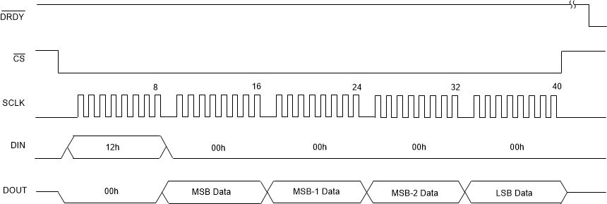
7.5.3.7 RDATA: Read Conversion Data Command
The RDATA command (Figure 7-25) is useful to re-read data within the same conversion period or to read data interrupted by a read register command. In both cases, DRDY is high because DRDY is driven high on the first SCLK of the previous operation. If DRDY is high, the first output byte is zero followed by data. If low, the first output byte is byte 1 of the conversion data, which is restarted for output byte 2.
 Figure 7-25 Read
Conversion Data by Command