SBASAW0 February 2024 ADS1288
PRODUCTION DATA
- 1
- 1 Features
- 2 Applications
- 3 Description
- 4 Pin Configuration and Functions
-
5 Specifications
- 5.1 Absolute Maximum Ratings
- 5.2 ESD Ratings
- 5.3 Recommended Operating Conditions
- 5.4 Thermal Information
- 5.5 Electrical Characteristics
- 5.6 Timing Requirements: 1.65V ≤ IOVDD ≤ 1.95V and 2.7V ≤ IOVDD ≤ 3.6V
- 5.7 Switching Characteristics: 1.65V ≤ IOVDD ≤ 1.95V and 2.7V ≤ IOVDD ≤ 3.6V
- 5.8 Timing Diagrams
- 5.9 Typical Characteristics
- 6 Parameter Measurement Information
-
7 Detailed Description
- 7.1 Overview
- 7.2 Functional Block Diagram
- 7.3 Feature Description
- 7.4 Device Functional Modes
- 7.5
Programming
- 7.5.1 Serial Interface
- 7.5.2 Conversion Data Format
- 7.5.3
Commands
- 7.5.3.1 Single Byte Command
- 7.5.3.2 WAKEUP: Wake Command
- 7.5.3.3 STANDBY: Software Power-Down Command
- 7.5.3.4 SYNC: Synchronize Command
- 7.5.3.5 RESET: Reset Command
- 7.5.3.6 Read Data Direct
- 7.5.3.7 RDATA: Read Conversion Data Command
- 7.5.3.8 RREG: Read Register Command
- 7.5.3.9 WREG: Write Register Command
- 7.5.3.10 OFSCAL: Offset Calibration Command
- 7.5.3.11 GANCAL: Gain Calibration Command
-
8 Register Map
- 8.1
Register Descriptions
- 8.1.1 ID/SYNC: Device ID, SYNC Register (Address = 00h) [Reset = xxxx0010b]
- 8.1.2 CONFIG0: Configuration Register 0 (Address = 01h) [Reset = 92h]
- 8.1.3 CONFIG1: Configuration Register 1 (Address = 02h) [Reset = 10h]
- 8.1.4 HPF0, HPF1: High-Pass Filter Registers (Address = 03h, 04h) [Reset = 32h, 03h]
- 8.1.5 OFFSET0, OFFSET1, OFFSET2: Offset Calibration Registers (Address = 05h, 06h, 07h) [Reset = 00h, 00h, 00h]
- 8.1.6 GAIN0, GAIN1, GAIN2: Gain Calibration Registers (Address = 08h, 09h, 0Ah) [Reset = 00h, 00h, 40h]
- 8.1.7 GPIO: Digital Input/Output Register (Address = 0Bh) [Reset = 000xx000b]
- 8.1.8 SRC0, SRC1: Sample Rate Converter Registers (Address = 0Ch, 0Dh) [Reset = 00h, 80h]
- 8.1
Register Descriptions
- 9 Application and Implementation
- 10Device and Documentation Support
- 11Revision History
- 12Mechanical, Packaging, and Orderable Information
Package Options
Mechanical Data (Package|Pins)
- RHB|32
Thermal pad, mechanical data (Package|Pins)
- RHB|32
Orderable Information
7.3.3 Voltage Reference Input
The ADC requires a reference voltage for operation. The reference voltage input is differential, defined as the voltage between the REFP and REFN pins: VREF = VREFP – VREFN. Because of the differential input, route the VREFN trace to the voltage reference ground terminal to avoid ground noise pickup. Use a precision 2.5V voltage reference with low noise, optimally less than 2μVRMS over the measurement bandwidth.
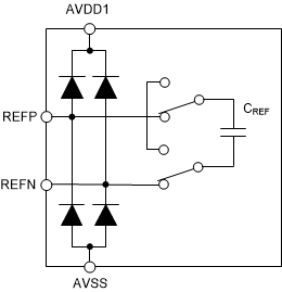
Figure 7-8 shows the simplified reference input circuit. Similar to the analog inputs, the reference inputs are protected by ESD diodes. If the reference inputs are driven below AVSS – 0.3V or above AVDD1 + 0.3V, the protection diodes can conduct. If these conditions are possible, use external clamp diodes, series resistors, or both to limit the reference input current to the specified value.
 Figure 7-8 Simplified Voltage Reference Input
Circuit
Figure 7-8 Simplified Voltage Reference Input
CircuitThe ADC samples the reference voltage by an internal capacitor (CREF) and then discharges the capacitor at the modulator sampling frequency (fMOD). The sampling operation results in transient current flow into the reference inputs. The transient current is filtered by a 0.1µF ceramic capacitor placed directly at the reference pins with a larger 10μF to 47μF capacitor at the voltage reference output. In applications where the voltage reference drives multiple ADCs, use 0.1µF capacitors at each ADC.
The external capacitors filter the current transients, resulting in 80μA/V average reference current. With VREF = 2.5V, the reference input current is 80μA / V × 2.5V = 200μA.