SBAS459K January 2010 – August 2015 ADS1294 , ADS1294R , ADS1296 , ADS1296R , ADS1298 , ADS1298R
PRODUCTION DATA.
- 1 Features
- 2 Applications
- 3 Description
- 4 Revision History
- 5 Device Comparison
- 6 Pin Configuration and Functions
- 7 Specifications
- 8 Parameter Measurement Information
-
9 Detailed Description
- 9.1 Overview
- 9.2 Functional Block Diagram
- 9.3
Feature Description
- 9.3.1
Analog Functionality
- 9.3.1.1 EMI Filter
- 9.3.1.2 Analog Input Structure
- 9.3.1.3
Input Multiplexer
- 9.3.1.3.1 Device Noise Measurements
- 9.3.1.3.2 Test Signals (TestP and TestN)
- 9.3.1.3.3 Auxiliary Differential Input (TESTP_PACE_OUT1, TESTN_PACE_OUT2)
- 9.3.1.3.4 Temperature Sensor (TempP, TempN)
- 9.3.1.3.5 Supply Measurements (MVDDP, MVDDN)
- 9.3.1.3.6 Lead-Off Excitation Signals (LoffP, LoffN)
- 9.3.1.3.7 Auxiliary Single-Ended Input
- 9.3.1.4 Analog Input
- 9.3.1.5 PGA Settings and Input Range
- 9.3.1.6 Reference
- 9.3.1.7
ECG-Specific Functions
- 9.3.1.7.1 Input Multiplexer (Rerouting The Right Leg Drive Signal)
- 9.3.1.7.2 Input Multiplexer (Measuring The Right Leg Drive Signal)
- 9.3.1.7.3 Wilson Central Terminal (WCT) and Chest Leads
- 9.3.1.7.4 Lead-Off Detection
- 9.3.1.7.5 RLD Lead-Off
- 9.3.1.7.6 Right Leg Drive (RLD) DC Bias Circuit
- 9.3.1.7.7 Pace Detect
- 9.3.1.7.8 Respiration
- 9.3.2 Digital Functionality
- 9.3.1
Analog Functionality
- 9.4 Device Functional Modes
- 9.5
Programming
- 9.5.1 SPI Interface
- 9.5.2
SPI Command Definitions
- 9.5.2.1 WAKEUP: Exit Standby Mode
- 9.5.2.2 STANDBY: Enter Standby Mode
- 9.5.2.3 RESET: Reset Registers to Default Values
- 9.5.2.4 START: Start Conversions
- 9.5.2.5 STOP: Stop Conversions
- 9.5.2.6 RDATAC: Read Data Continuous
- 9.5.2.7 SDATAC: Stop Read Data Continuous
- 9.5.2.8 RDATA: Read Data
- 9.5.2.9 Sending Multibyte Commands
- 9.5.2.10 RREG: Read From Register
- 9.5.2.11 WREG: Write to Register
- 9.6
Register Maps
- 9.6.1
Register Descriptions
- 9.6.1.1 ID: ID Control Register (address = 00h) (reset = xxh)
- 9.6.1.2 CONFIG1: Configuration Register 1 (address = 01h) (reset = 06h)
- 9.6.1.3 CONFIG2: Configuration Register 2 (address = 02h) (reset = 40h)
- 9.6.1.4 CONFIG3: Configuration Register 3 (address = 03h) (reset = 40h)
- 9.6.1.5 LOFF: Lead-Off Control Register (address = 04h) (reset = 00h)
- 9.6.1.6 CHnSET: Individual Channel Settings (n = 1 to 8) (address = 05h to 0Ch) (reset = 00h)
- 9.6.1.7 RLD_SENSP: RLD Positive Signal Derivation Register (address = 0Dh) (reset = 00h)
- 9.6.1.8 RLD_SENSN: RLD Negative Signal Derivation Register (address = 0Eh) (reset = 00h)
- 9.6.1.9 LOFF_SENSP: Positive Signal Lead-Off Detection Register (address = 0Fh) (reset = 00h)
- 9.6.1.10 LOFF_SENSN: Negative Signal Lead-Off Detection Register (address = 10h) (reset = 00h)
- 9.6.1.11 LOFF_FLIP: Lead-Off Flip Register (address = 11h) (reset = 00h)
- 9.6.1.12 LOFF_STATP: Lead-Off Positive Signal Status Register (address = 12h) (reset = 00h)
- 9.6.1.13 LOFF_STATN: Lead-Off Negative Signal Status Register (address = 13h) (reset = 00h)
- 9.6.1.14 GPIO: General-Purpose I/O Register (address = 14h) (reset = 0Fh)
- 9.6.1.15 PACE: Pace Detect Register (address = 15h) (reset = 00h)
- 9.6.1.16 RESP: Respiration Control Register (address = 16h) (reset = 00h)
- 9.6.1.17 CONFIG4: Configuration Register 4 (address = 17h) (reset = 00h)
- 9.6.1.18 WCT1: Wilson Central Terminal and Augmented Lead Control Register (address = 18h) (reset = 00h)
- 9.6.1.19 WCT2: Wilson Central Terminal Control Register (address = 18h) (reset = 00h)
- 9.6.1
Register Descriptions
- 10Application and Implementation
- 11Power Supply Recommendations
- 12Layout
- 13Device and Documentation Support
- 14Mechanical, Packaging, and Orderable Information
Package Options
Mechanical Data (Package|Pins)
Thermal pad, mechanical data (Package|Pins)
- PAG|64
Orderable Information
10 Application and Implementation
NOTE
Information in the following applications sections is not part of the TI component specification, and TI does not warrant its accuracy or completeness. TI’s customers are responsible for determining suitability of components for their purposes. Customers should validate and test their design implementation to confirm system functionality.
10.1 Application Information
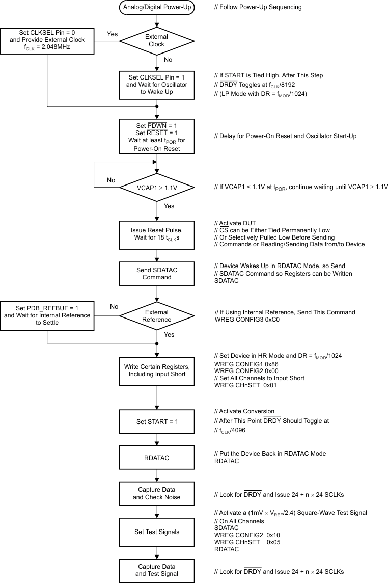
10.1.1 Setting the Device for Basic Data Capture
Figure 93 outlines the procedure to configure the device in a basic state and capture data. This procedure puts the device into a configuration that matches the parameters listed in the Specifications section, in order to check if the device is working properly in the user system. Follow this procedure initially until familiar with the device settings. After this procedure has been verified, the device can be configured as needed. For details on the timings for commands, refer to the appropriate sections in the data sheet. Sample programming codes are added for the ECG-specific functions.
10.1.1.1 Lead-Off
Sample code to set dc lead-off with pullup or pulldown resistors on all channels:
WREG LOFF 0x13       // Comparator threshold at 95% and 5%, pullup or pulldown resistor
                     // dc lead-off
WREG CONFIG4    0x02 // Turn on dc lead-off comparators
WREG LOFF_SENSP 0xFF // Turn on the P-side of all channels for lead-off sensing
WREG LOFF_SENSN 0xFF // Turn on the N-side of all channels for lead-off sensing
Observe the status bits of the output data stream to monitor lead-off status.
10.1.1.2 Right Leg Drive
Sample code to choose RLD as an average of the first three channels.
WREG RLD_SENSP 0x07        // Select channel 1-3 P-side for RLD sensing
WREG RLD_SENSN 0x07        // Select channel 1-3 N-side for RLD sensing
WREG CONFIG3   b’x1xx 1100 // Turn on RLD amplifier, set internal RLDREF voltage
Sample code to route the RLD_OUT signal through channel 4 N-side and measure RLD with channel 5. Make sure the external side to the chip RLDOUT is connected to RLDIN.
WREG CONFIG3 b’xxx1 1100  // Turn on RLD amp, set internal RLDREF voltage, set RLD measurement bit
WREG CH4SET  b’1xxx 0111  // Route RLDIN to channel 4 N-side
WREG CH5SET  b’1xxx 0010  // Route RLDIN to be measured at channel 5 w.r.t RLDREF
10.1.1.3 Pace Detection
Sample code to select channel 5 and 6 outputs for pace:
WREG PACE b’0001 0101 // Power-up pace amplifier and select channel 5 and 6 for pace out
10.1.2 Establishing the Input Common-Mode
The ADS129x measures fully-differential signals where the common-mode voltage point is the midpoint of the positive and negative analog input. The internal PGA restricts the common-mode input range because of the headroom required for operation. The human body is prone to common-mode drifts because noise easily couples onto the human body, similar to an antenna. These common-mode drifts may push the ADS129x input common-mode voltage out of the measurable range of the ADC.
If a patient-drive electrode is used by the system, the ADS129x includes an on-chip right leg drive (RLD) amplifier that connects to the patient drive electrode. The RLD amplifier function is to bias the patient to maintain the other electrode common-mode voltages within the valid range. When powered on, the amplifier uses either the analog midsupply voltage, or the voltage present at the RLDREF pin, as a reference input to stabilize the output near that voltage.
The ADS129x provide the option to use input electrode voltages as feedback to the amplifier to more effectively stabilize the output to the amplifier reference voltage by setting corresponding bits in the RLD_SENSP and RLD_SENSN registers. See to Figure 94 for an example of a three-electrode system that leverages this technique.
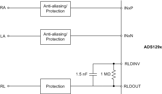 Figure 94. Setting Common-Mode Using RLD Electrode
A second strategy for maintaining a valid common-mode voltage is to ac-couple the analog inputs, which is especially useful when a patient-drive electrode is not in use. A dc blocking capacitor combined with a voltage divider between the analog power supplies, or a pullup resistor to set the DC bias to a known point, effectively makes sure that the dc common-mode voltage never drifts. Applications that do not use a patient-drive electrode may still use the RLD amplifier on the ADS129x as a buffered midsupply voltage to bias the inputs. Take care when choosing the passive components because the capacitor and the resistors form an RC high-pass filter. If passive components are chosen poorly, the filter undesirably attenuates frequencies at the lower end of the signal band. Figure 95 shows an example of this configuration.
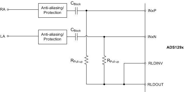 Figure 95. Setting Common-Mode Without Using RLD Electrode
10.1.3 Antialiasing
As with all analog-to-digital systems, take care to prevent undesired aliasing effects. The ADS129x modulator samples the input at either 256 kHz or 512 kHz, depending on whether the device is in low-power (LP) mode or high-resolution (HR) mode, respectively. As is the case with all digital filters, the response of the on-chip digital decimation filter on the ADS129x repeats at integer multiples of the modulator frequency. A benefit to using the delta-sigma architecture is that the digital decimation filter significantly attenuates frequencies between the signal band and the alias of the signal band near the modulator frequency. This attenuation, combined with the limited bandwidth of the PGA (see Table 5), makes the requirement on the steepness of the response of the analog antialiasing filter much less stringent. In many cases, acceptable attenuation at the modulator frequency is provided by either a single or double-pole RC low pass filter.
Also take care when choosing components for antialiasing. Common-mode to differential-mode conversion as a result of component mismatch, including antialiasing components, causes common-mode rejection degradation. Figure 96 shows a typical front-end configuration.
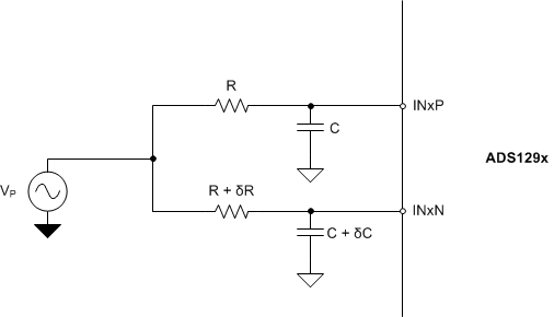 Figure 96. Typical Front-End Configuration
VP is the common-mode signal to the system. If the values of R and C modeled in the differential signal are perfectly matched, then the system exhibits a very large CMR. If δR and δC in resistor R and capacitor C, respectively, are mismatched, the CMR of the entire system is approximated to Equation 8.

where
- fC is the –3-dB frequency of the RC filter.
If 1%-precision external components are used and the bandwidth of the RC filter is approximately 6 kHz, the system then has only 74 dB of CMR at 60 Hz. In the real world, the front-end of the ECG does not contain only first-order RC filters; electrodes, cables, and second- or third-order RC filters are also included. Considering all of these components, mismatch can easily accumulate, and thus contribute up to 20% or more of the signal. This degree of mismatch degrades the CMR of the system to less than 60 dB at 60 Hz. Therefore, it is necessary to consider different techniques to improve CMR.
There is a tradeoff when placing the bandwidth of the antialiasing filter in front of the modulator. Considering the mismatch between the discrete components, it is better to select the large bandwidth; the upper limit of the bandwidth is determined by the sampling frequency of the modulator. For more information on ways to prevent common-mode rejection, see Improving Common-Mode Rejection Using the Right-Leg Drive Amplifier, SBAA188.
10.2 Typical Applications
10.2.1 ADS129xR Respiration Measurement Using Internal Modulation Circuitry
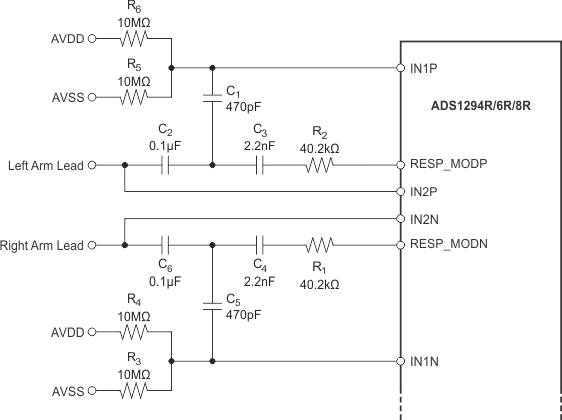
The respiration measurement circuitry on the ADS129xR employs out-of-band amplitude modulation and demodulation to measure changes in thoracic impedance that correspond to breathing. When respiration mode is enabled, channel 1 cannot be used to acquire ECG signals because the internal demodulation circuitry is unique to that channel. ECG signals can still be acquired with the same electrodes used for respiration measurement if they are also connected to another channel. Note the configuration shown in Figure 97.
10.2.1.1 Design Requirements
Table 36 shows the design requirements for the components shown in Figure 97.
Table 36. Respiration Design Requirements
| DESIGN PARAMETER | VALUE |
|---|---|
| Modulation frequency | 32 kHz or 64 kHz |
| Input high-pass filter cutoff | ≈ 68 Hz |
| ADC reference voltage | 2.4 V |
| Maximum ac body current | 100 μA |
| Minimum resistance R1 + R2 | 24 kΩ |
10.2.1.2 Detailed Design Procedure
To configure the ADS129xR to use its internal modulation circuitry, set RESP register bits[6:7] to enable both the internal modulation and demodulation circuitry. RESP register bits[4:2] determine the phase of the demodulation blocking signal. To configure the device to use the internally generated signals for internal respiration measurement, configure RESP register bits[1:0] to 10b.
The RESP_MODP and RESP_MODN pins produce a 32 kHz or 64 kHz square wave depending on the CONFIG4 regsiter bits[7:5] when configured to use the internal circuitry. The REP_MODP and RESP_MODN pin voltages toggle between VREFP and VREFN at opposite phases at the specified frequency.
Choosing R1 and R2 involves first recognizing the ideal behavior of this circuit. Ideally, all of the series capacitors appear as short-circuits to the high-frequency modulation signal, and there is no nonideal shunt capacitance anywhere in the circuit. Figure 98 shows an equivalent circuit representing these assumptions.
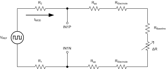 Figure 98. Ideal Behavior of the Respiration Modulation Circuit.
The voltage appearing at the channel 1 input is set by the voltage divider formed by the resistors in the circuit. Resistor RPP represents any patient protection resistance in the cable; RElectrode represents the electrode-to-body interface resistance; RBaseline represents the baseline body impedance; and ΔR is the change in thoracic impedance due to respiration. Assume that R1 and R2 are significantly larger than all the other resistors in the circuit, and then approximate the RESP_MOD pins as the terminals of an ac current source with magnitude IMOD according to Equation 9:

where
- VREF is the square wave with the amplitude VREFP – VREFN that is produced at the RESP_MOD pins.
According to IEC60601, patient current at a frequency of 32 kHz must be limited to less than 100 μA; this limitation places a minimum value on the combination of R1 and R2.
For best performance, the inputs to the ADS129xR must be ac coupled and biased to midsupply. The components that perform this function correspond to C1, C5, R3, R4, R5, and R6 in Figure 97. It is possible for ECG interference to couple into channel 1. As a result of this possibility, it is advisable to make the high-pass filter cutoff of those components large enough to attenuate the ECG bandwidth significantly. Conversely, if the cutoff is set to high, the carrier signal may attenuate.
The signal that appears at the channel 1 input is amplified by the PGA, and then fed to the internal demodulation block. The demodulation block removes the square wave from the input leaving only the very low-frequency waveform corresponding to the ΔR due to respiration, and the offset due to RPP, RElectrode, and RBaseline. Equation 10 describes the modulator output voltage corresponding to the change in body impedance.

Measure the rate of respiration by using the period at which VRESP oscillates as a result of ΔR. Make sure that the magnitude of VRESP remains greater than the noise-free resolution of the ADS129x. This magnitude imposes upper limits on the sizes of R1 and R2, as well as the cable impedance RPP, and demands that the quality of the electrode-to-body connection is high.
Parasitic shunt capacitance tends to attenuate high frequencies and the outputs from the PGA are limited by the bandwidth of the amplifiers. The result is that the square edges of the carrier are rounded. To account for this error, the ADS129xR allows configuration of the RESP_PH[2:0] bits in the RESP regsiter. Those bits control the demodulation phase that introduces a phase delay between the modulation and demodulation clocks to account for the delay introduced by low-pass elements in the circuit.
Choosing the optimal phase depends on the system characteristics. The time constant introduced by the resistance in the path of the input and the cable capacitance is an example of a system level characteristic that influences the amount of phase required for optimal respiration rate measurement.
Figure 99 shows a respiration test circuit. Figure 100 and Figure 101 plot noise on channel 1 for the ADS129xR as baseline impedance, gain, and phase are swept. The x-axis is the baseline impedance, normalized to a 29-μA modulation current (see Equation 11).
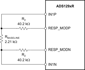 Figure 99. Respiration-Noise Test Circuit
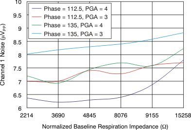
| BW = 150 Hz, respiration modulation clock = 32 kHz |
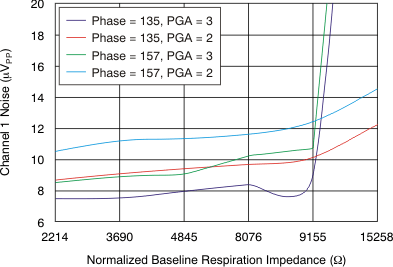
| BW = 150 Hz, respiration modulation clock = 64 kHz |

where
- RACTUAL is the baseline body impedance.
- IACTUAL is the modulation current, as calculated by (VREFP – VREFN) divided by the impedance of the modulation circuit.
For example, assume that:
- Modulation frequency = 32 kHz
- RACTUAL = 3 kΩ
- IACTUAL = 50 μA
- RNORMALIZED = (3 kΩ × 50 μA) / 29 μA = 5.1 kΩ
Referring to Figure 100 and Figure 101, gain = 4 and phase = 112.5° yield the best performance at 6.4 μVPP. Low-pass filtering this signal with a high-order, 2-Hz cutoff reduces the noise to less than 600 nVPP. The impedance resolution is 600 nVPP / 29 μA = 20 mΩ. When the modulation frequency is 32 kHz, use gains of 3 and 4, and a phase of 112.5° and 135° for best performance. When the modulation frequency is 64 kHz, use gains of 2 and 3 and phase of 135° and 157° for best performance.
10.2.1.3 Application Curve
Figure 102 shows respiration data taken with the ADS1298RECGFE-PDK using the Fluke medSim 300b. The data was then low-pass filtered to attenuate noise outside of the band of interest. A modulation frequency of
32 kHz was used along with a PGA gain of 3 and a RESP_PH setting of 112.5°.
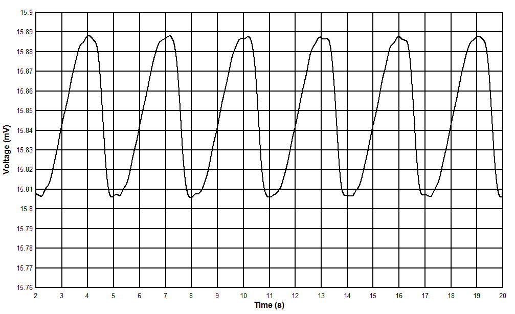 Figure 102. Respiration Impedance Taken With ADS1298R
10.2.2 Software-Based Artificial Pacemaker Detection Using the PACEOUT Pins on the ADS129x
The electrical pulses produced by an artificial pacemaker are used to regulate the beating of the heart, and have a very small duration (width) when measured on the scale of other biopotential signals. According to the standard listed in AAMI EC11, medical instrumentation must be capable of capturing pacemaker pulses with durations as narrow as 0.5 ms. The ADS129x is capable of capturing data at 32 kSPS; ideally, fast enough to capture even the narrowest pulse. However, the data rate setting on the ADS129x is global for all channels. Using the ADS129x to digitize an input channel fast enough for robust pacemaker detection dictates that all channels must be converted as quickly; a condition that may be undesirable.
An alternative topology is to use the ADS129x internal pace buffers to route a single-ended version of any particular channel input out to a fast-sampling SAR ADC to digitize the detection channel signal separately. Detection of a pacemaker pulse is then performed in the digital domain. Refer to Figure 103 for the basic block diagram for this architecture. The example features the combination of the OPA320 and the ADS7042. The OPA320 is used to drive the input sampling structure of the ADS7042, but provides corollary flexibility to add another gain stage and active antialias filtering before the pace output is digitized.
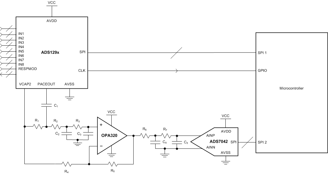 Figure 103. Block Diagram of the Software Pacemaker Detection Topology
10.2.2.1 Design Requirements
Table 37 shows the design requirements for the components shown in Figure 103.
Table 37. Software Pace Design Requirements
| DESIGN PARAMETER | VALUE |
|---|---|
| Analog supply voltage | 3.3 V |
| Minimum pacemaker signal bandwidth | 0.5 ms |
| Minimum pacemaker signal amplitude | 2 mV |
| Feedback network R4 + R5 (nonunity gain) | ≈ 100 kΩ |
10.2.2.2 Detailed Design Procedure
The pace amplifiers on the ADS129x provides differential to single-ended conversion and amplification of 0.4 V/V to whatever voltage appears at the output of the PGA of the channel from which the pace amplifier is routed. Selecting which channels are routed to the pace amplifiers is performed in the pace detect register of the ADS129x. The voltage that appears at the output of the pace amplifier is to be taken with respect to analog midsupply.
Before the signal is converted by the ADS7042, the signal must be buffered by a high-speed op amp because the inputs of the ADS7042 represent a switch-capacitor type load. The OPA320 is ideal to perform this function because of the low input bias current and 20-MHz unity gain bandwidth. The op amp also provides the flexibility to provide an extra gain stage before the SAR ADC, isolate filter stages, or to provide simple buffering. The purpose of C1 and R1 are to provide ac coupling to the pacemaker detection signal. This coupling may be necessary because electrode offset and the pacemaker pulse can both be, in some cases, up to a few hundred millivolts.
An actively-driven signal ground is required to set the dc bias of the op amp at midsupply. It is possible to use the voltage provided at VCAP2 on the ADS129x as a buffered midsupply voltage. The voltage at the VCAP2 pin may be noisy, but using it to drive the common-mode voltage for both inverting and noninverting inputs to the op amp causes the op amp to cancel that noise significantly because it is common to both inputs.
Op amp feedback resistors R4 and R5 set the gain for the OPA320. The transfer function for this configuration is that of the noninverting op amp configuration shown in Equation 12.

Resistors R4 and R5 are chosen to set the desired gain. The series combination is approximately 100 kΩ, so that both the feedback current is limited to within the ADS129x VCAP2 internal regulator drive strength, and the Johnson-Nyquist noise of the resistors remains negligible.
If the OPA320 is to be used only as a buffer, remove R4 removed to provide unity gain. If ac coupling is not desired, for best performance, replace C1 with a 0-Ω resistor and depopulate R1.
The RC network of R2, C2, R3, C3, R6, C4, R7, and C5 form isolated two-pole RC antialiasing filters for the SAR ADC. The component values of the filter are set to provide significant attenuation at the ADC sampling frequency, but still provide enough bandwidth to detect a pacemaker pulse. A bandwidth of greater than 2 kHz is enough to capture a narrow 0.5-ms pacemaker pulse.
In a real-time system, data must be collected and analyzed for a pacemaker with each incoming sample. Digitally filter data that are collected from the ADS7042 to remove out-of-band noise. Unlike a delta-sigma converter, a SAR converter does not apply a filter to the data before it is sent to the host. There are a number of factors that drive a decision on digital-filter implementation. Some of those factors include steepness of the response, phase linearity, and the number of taps. When using this topology with an ADS129xR device simultaneously with the respiration measurement circuitry, take special care to remove noise generated by the respiration modulation circuitry.
The key to detecting a pacemaker pulse is the detection of a steep transition in the input voltage. To measure the magnitude of the transitions in input voltages, apply a digital differentiator algorithm. The algorithm measures the change in voltage magnitude over the span of a few samples and compares the change to a threshold required to trigger detection. The following pseudocode exemplifies some of the processing steps required to use this topology:
newDataPoint = collectFromADS7042( );            // Collect data from the ADS7042
                                                 // Apply combined low-pass filter and differentiator
inputRateOfChange = LPFandDifferentiator( newDataPoint );
if( abs( inputRateOfChange ) > thresholdValue )  // Check if a quick edge occurred
{
pacemakerFlag = true;                            // Edge detected
}
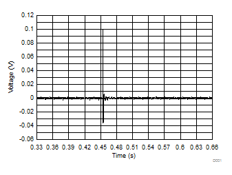
10.2.2.3 Application Curve
Figure 104 shows data that was collected from the PACEOUT pin of the ADS1298R (using the OPA320 and the ADS7042), and then filtered. The pacemaker pulse can be clearly identified.
