SBAS590E March 2016 – June 2020 ADS131A02 , ADS131A04
PRODUCTION DATA.
- 1 Features
- 2 Applications
- 3 Description
- 4 Revision History
- 5 Device Comparison Table
- 6 Pin Configuration and Functions
-
7 Specifications
- 7.1 Absolute Maximum Ratings
- 7.2 ESD Ratings
- 7.3 Recommended Operating Conditions
- 7.4 Thermal Information
- 7.5 Electrical Characteristics
- 7.6 Timing Requirements: Asynchronous Interrupt Interface Mode
- 7.7 Switching Characteristics: Asynchronous Interrupt Interface Mode
- 7.8 Timing Requirements: Synchronous Master Interface Mode
- 7.9 Switching Characteristics: Synchronous Master Interface Mode
- 7.10 Timing Requirements: Synchronous Slave Interface Mode
- 7.11 Switching Characteristics: Synchronous Slave Interface Mode
- 7.12 Typical Characteristics
- 8 Parameter Measurement Information
-
9 Detailed Description
- 9.1 Overview
- 9.2 Functional Block Diagram
- 9.3 Feature Description
- 9.4 Device Functional Modes
- 9.5
Programming
- 9.5.1 Interface Protocol
- 9.5.2 SPI Interface
- 9.5.3
SPI Command Definitions
- 9.5.3.1 NULL: Null Command
- 9.5.3.2 RESET: Reset to POR Values
- 9.5.3.3 STANDBY: Enter Standby Mode
- 9.5.3.4 WAKEUP: Exit Standby Mode
- 9.5.3.5 LOCK: Lock ADC Registers
- 9.5.3.6 UNLOCK: Unlock ADC Registers
- 9.5.3.7 RREG: Read a Single Register
- 9.5.3.8 RREGS: Read Multiple Registers
- 9.5.3.9 WREG: Write Single Register
- 9.5.3.10 WREGS: Write Multiple Registers
- 9.6
Register Maps
- 9.6.1
User Register Description
- 9.6.1.1 ID_MSB: ID Control Register MSB (address = 00h) [reset = xxh]
- 9.6.1.2 ID_LSB: ID Control Register LSB (address = 01h) [reset = xxh]
- 9.6.1.3 STAT_1: Status 1 Register (address = 02h) [reset = 00h]
- 9.6.1.4 STAT_P: Positive Input Fault Detect Status Register (address = 03h) [reset = 00h]
- 9.6.1.5 STAT_N: Negative Input Fault Detect Status Register (address = 04h) [reset = 00h]
- 9.6.1.6 STAT_S: SPI Status Register (address = 05h) [reset = 00h]
- 9.6.1.7 ERROR_CNT: Error Count Register (address = 06h) [reset = 00h]
- 9.6.1.8 STAT_M2: Hardware Mode Pin Status Register (address = 07h) [reset = xxh]
- 9.6.1.9 Reserved Registers (address = 08h to 0Ah) [reset = 00h]
- 9.6.1.10 A_SYS_CFG: Analog System Configuration Register (address = 0Bh) [reset = 60h]
- 9.6.1.11 D_SYS_CFG: Digital System Configuration Register (address = 0Ch) [reset = 3Ch]
- 9.6.1.12 CLK1: Clock Configuration 1 Register (address = 0Dh) [reset = 08h]
- 9.6.1.13 CLK2: Clock Configuration 2 Register (address = 0Eh) [reset = 86h]
- 9.6.1.14 ADC_ENA: ADC Channel Enable Register (address = 0Fh) [reset = 00h]
- 9.6.1.15 Reserved Register (address = 10h) [reset = 00h]
- 9.6.2 ADCx: ADC Channel Digital Gain Configuration Registers (address = 11h to 14h) [reset = 00h]
- 9.6.1
User Register Description
- 10Application and Implementation
- 11Power Supply Recommendations
- 12Layout
- 13Device and Documentation Support
- 14Mechanical, Packaging, and Orderable Information
Package Options
Refer to the PDF data sheet for device specific package drawings
Mechanical Data (Package|Pins)
- PBS|32
Thermal pad, mechanical data (Package|Pins)
- PBS|32
Orderable Information
9.3.2 Analog Input
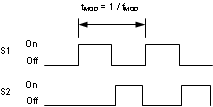
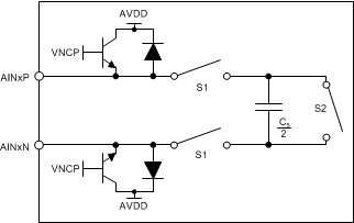
The ADS131A0x analog inputs are directly connected to the switched-capacitor sampling network of the ΔΣ modulator without a multiplexer or integrated buffer. The device inputs are measured differentially (VIN = VAINxP – VAINxN) and can span from –VREF / Gain to VREF / Gain. Figure 38 shows a conceptual diagram of the modulator circuit charging and discharging the sampling capacitor through switches, although the actual implementation is slightly different. The timing for switches S1 and S2, as shown in Figure 37, are 180 degrees out-of-phase of one another.
 Figure 37. S1 and S2 Switch Timing
 Electrostatic discharge (ESD) circuitry protects the inputs. Figure 38 shows a simplified representation of the ESD circuit. Protection for input voltages exceeding AVDD can be modeled as a simple diode.
The negative charge pump voltage, VNCP, controls the voltage at which the low-side protection devices begin conducting. Tie VNCP to AVSS if the charge pump is not used to ensure the clamping voltage is properly set. The charge pump cannot provide a large amount of current. The mechanism shown in Figure 38 ensures current provided by the charge pump is limited in the case of an overvoltage event.
To prevent the ESD diodes from being enabled, the absolute voltage on any input must stay within the range provided by Equation 3 when the internal charge pump is disabled and within the range in Equation 4 when the internal charge pump is enabled:
If the voltages on the input pins have any potential to violate these conditions, external clamp diodes or series resistors may be required to limit the input currents to safe values (see the Absolute Maximum Ratings table).
The charging of the input capacitors draws a transient current from the sensor driving the ADS131A0x inputs. The average value of this current can be used to calculate an effective impedance of ZIN, where ZIN = VIN / IAVERAGE. This effective input impedance is a function of the modulator sampling frequency and Equation 5 can be used to calculate an estimate value. When using fMOD = 4.096 MHz, the input impedance is approximately 130 kΩ.

where
- fMOD = modulator clock and
- CS = 3.5 pF
There are two general methods of driving the ADS131A0x analog inputs, as shown in Figure 39: pseudo-differential or fully-differential.
 Figure 39. Pseudo-Differential and Fully-Differential Inputs
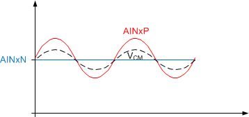
 To apply a pseudo-differential signal to the fully-differential inputs, apply a dc voltage to AINxN, preferably to the analog mid-supply [(AVDD + AVSS) / 2] or [(AVDD + VNCP) / 2] when the negative charge pump is enabled. The AINxP pins can swing between –VREF / Gain to VREF / Gain (as shown in Figure 40) around the common voltage. The common-mode voltage, VCM, changes with VAINxP.
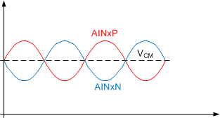
Configure the signals at AINxP and AINxN to be 180° out-of-phase centered around a common-mode voltage to use a fully-differential input method. Both the AINxP and AINxN inputs swing from VCM +½ VREF / Gain to VCM –½ VREF / Gain, as shown in Figure 41. The differential voltage at the maximum and minimum points is equal to VREF / Gain to –VREF / Gain, respectively. The VCM voltage remains fixed when AINxP and AINxN swing. Use the ADS131A0x in a differential configuration to maximize the dynamic range of the data converter. For optimal performance, the VCM is recommended to be set at the midpoint of the analog supplies.
Tie any unused analog input channels directly to AVSS.
 Figure 40. Pseudo-Differential Input Mode
  Figure 41. Fully-Differential Input Mode