SBAS590E March   2016  – June 2020 ADS131A02 , ADS131A04

PRODUCTION DATA.  

  1. Features
  2. Applications
  3. Description
    1.     Simplified Block Diagram
  4. Revision History
  5. Device Comparison Table
  6. Pin Configuration and Functions
    1.     Pin Functions
  7. Specifications
    1. 7.1  Absolute Maximum Ratings
    2. 7.2  ESD Ratings
    3. 7.3  Recommended Operating Conditions
    4. 7.4  Thermal Information
    5. 7.5  Electrical Characteristics
    6. 7.6  Timing Requirements: Asynchronous Interrupt Interface Mode
    7. 7.7  Switching Characteristics: Asynchronous Interrupt Interface Mode
    8. 7.8  Timing Requirements: Synchronous Master Interface Mode
    9. 7.9  Switching Characteristics: Synchronous Master Interface Mode
    10. 7.10 Timing Requirements: Synchronous Slave Interface Mode
    11. 7.11 Switching Characteristics: Synchronous Slave Interface Mode
    12. 7.12 Typical Characteristics
  8. Parameter Measurement Information
    1. 8.1 Noise Measurements
  9. Detailed Description
    1. 9.1 Overview
    2. 9.2 Functional Block Diagram
    3. 9.3 Feature Description
      1. 9.3.1 Clock
        1. 9.3.1.1 XTAL1/CLKIN and XTAL2
        2. 9.3.1.2 ICLK
        3. 9.3.1.3 MODCLK
        4. 9.3.1.4 Data Rate
      2. 9.3.2 Analog Input
      3. 9.3.3 Input Overrange and Underrange Detection
      4. 9.3.4 Reference
      5. 9.3.5 ΔΣ Modulator
      6. 9.3.6 Digital Decimation Filter
      7. 9.3.7 Watchdog Timer
    4. 9.4 Device Functional Modes
      1. 9.4.1 Low-Power and High-Resolution Mode
      2. 9.4.2 Power-Up
      3. 9.4.3 Standby and Wake-Up Mode
      4. 9.4.4 Conversion Mode
      5. 9.4.5 Reset (RESET)
    5. 9.5 Programming
      1. 9.5.1 Interface Protocol
        1. 9.5.1.1 Device Word Length
        2. 9.5.1.2 Fixed versus Dynamic-Frame Mode
        3. 9.5.1.3 Command Word
        4. 9.5.1.4 Status Word
        5. 9.5.1.5 Data Words
          1. 9.5.1.5.1 ADC Data Word 16-Bit Format
          2. 9.5.1.5.2 ADC Data Word 24-Bit Format
        6. 9.5.1.6 Hamming Code Error Correction
        7. 9.5.1.7 Cyclic Redundancy Check (CRC)
          1. 9.5.1.7.1 Computing the CRC
          2. 9.5.1.7.2 CRC With CRC_MODE = 1
          3. 9.5.1.7.3 CRC with CRC_MODE = 0
          4. 9.5.1.7.4 CRC Using the WREGS Command
      2. 9.5.2 SPI Interface
        1. 9.5.2.1 Asynchronous Interrupt Mode
          1. 9.5.2.1.1 Chip Select (CS)
          2. 9.5.2.1.2 Serial Clock (SCLK)
          3. 9.5.2.1.3 Data Input (DIN)
          4. 9.5.2.1.4 Data Output (DOUT)
          5. 9.5.2.1.5 Data Ready (DRDY)
          6. 9.5.2.1.6 Asynchronous Interrupt Mode Data Retrieval
        2. 9.5.2.2 Synchronous Master Mode
          1. 9.5.2.2.1 Serial Clock (SCLK)
          2. 9.5.2.2.2 Data Input (DIN)
          3. 9.5.2.2.3 Data Output (DOUT)
          4. 9.5.2.2.4 Data Ready (DRDY)
          5. 9.5.2.2.5 Chip Select (CS)
          6. 9.5.2.2.6 Synchronous Master Mode Data Retrieval
        3. 9.5.2.3 Synchronous Slave Mode
          1. 9.5.2.3.1 Chip Select (CS)
          2. 9.5.2.3.2 Serial Clock (SCLK)
          3. 9.5.2.3.3 Data Input (DIN)
          4. 9.5.2.3.4 Data Output (DOUT)
          5. 9.5.2.3.5 Data Ready (DRDY)
          6. 9.5.2.3.6 Synchronous Slave Mode Data Retrieval
        4. 9.5.2.4 ADC Frame Complete (DONE)
      3. 9.5.3 SPI Command Definitions
        1. 9.5.3.1  NULL: Null Command
        2. 9.5.3.2  RESET: Reset to POR Values
        3. 9.5.3.3  STANDBY: Enter Standby Mode
        4. 9.5.3.4  WAKEUP: Exit Standby Mode
        5. 9.5.3.5  LOCK: Lock ADC Registers
        6. 9.5.3.6  UNLOCK: Unlock ADC Registers
          1. 9.5.3.6.1 UNLOCK from POR or RESET
        7. 9.5.3.7  RREG: Read a Single Register
        8. 9.5.3.8  RREGS: Read Multiple Registers
        9. 9.5.3.9  WREG: Write Single Register
        10. 9.5.3.10 WREGS: Write Multiple Registers
    6. 9.6 Register Maps
      1. 9.6.1 User Register Description
        1. 9.6.1.1  ID_MSB: ID Control Register MSB (address = 00h) [reset = xxh]
          1. Table 16. ID_MSB Register Field Descriptions
        2. 9.6.1.2  ID_LSB: ID Control Register LSB (address = 01h) [reset = xxh]
          1. Table 17. ID_LSB Register Field Descriptions
        3. 9.6.1.3  STAT_1: Status 1 Register (address = 02h) [reset = 00h]
          1. Table 18. STAT_1 Register Field Descriptions
        4. 9.6.1.4  STAT_P: Positive Input Fault Detect Status Register (address = 03h) [reset = 00h]
          1. Table 19. STAT_P Register Field Descriptions
        5. 9.6.1.5  STAT_N: Negative Input Fault Detect Status Register (address = 04h) [reset = 00h]
          1. Table 20. STAT_N Register Field Descriptions
        6. 9.6.1.6  STAT_S: SPI Status Register (address = 05h) [reset = 00h]
          1. Table 21. STAT_S Register Field Descriptions
        7. 9.6.1.7  ERROR_CNT: Error Count Register (address = 06h) [reset = 00h]
          1. Table 22. ERROR_CNT Register Field Descriptions
        8. 9.6.1.8  STAT_M2: Hardware Mode Pin Status Register (address = 07h) [reset = xxh]
          1. Table 23. STAT_M2 Register Field Descriptions
        9. 9.6.1.9  Reserved Registers (address = 08h to 0Ah) [reset = 00h]
          1. Table 24. Reserved Registers Field Descriptions
        10. 9.6.1.10 A_SYS_CFG: Analog System Configuration Register (address = 0Bh) [reset = 60h]
          1. Table 25. A_SYS_CFG Register Field Descriptions
        11. 9.6.1.11 D_SYS_CFG: Digital System Configuration Register (address = 0Ch) [reset = 3Ch]
          1. Table 27. D_SYS_CFG Register Field Descriptions
        12. 9.6.1.12 CLK1: Clock Configuration 1 Register (address = 0Dh) [reset = 08h]
          1. Table 28. CLK1 Register Field Descriptions
        13. 9.6.1.13 CLK2: Clock Configuration 2 Register (address = 0Eh) [reset = 86h]
          1. Table 29. CLK2 Register Field Descriptions
        14. 9.6.1.14 ADC_ENA: ADC Channel Enable Register (address = 0Fh) [reset = 00h]
          1. Table 31. ADC_ENA Register Field Descriptions
        15. 9.6.1.15 Reserved Register (address = 10h) [reset = 00h]
          1. Table 32. Reserved Register Field Descriptions
      2. 9.6.2 ADCx: ADC Channel Digital Gain Configuration Registers (address = 11h to 14h) [reset = 00h]
        1. Table 33. ADCx Registers Field Descriptions
  10. 10Application and Implementation
    1. 10.1 Application Information
      1. 10.1.1 Unused Inputs and Outputs
      2. 10.1.2 Power Monitoring Specific Applications
      3. 10.1.3 Multiple Device Configuration
        1. 10.1.3.1 First Device Configured in Asynchronous Interrupt Mode
        2. 10.1.3.2 First Device Configured in Synchronous Master Mode
        3. 10.1.3.3 All Devices Configured in Synchronous Slave Mode
    2. 10.2 Typical Application
      1. 10.2.1 Design Requirements
      2. 10.2.2 Detailed Design Procedure
      3. 10.2.3 Application Curve
    3. 10.3 What To Do and What Not To Do
    4. 10.4 Initialization Set Up
  11. 11Power Supply Recommendations
    1. 11.1 Negative Charge Pump
    2. 11.2 Internal Digital LDO
    3. 11.3 Power-Supply Sequencing
    4. 11.4 Power-Supply Decoupling
  12. 12Layout
    1. 12.1 Layout Guidelines
    2. 12.2 Layout Example
  13. 13Device and Documentation Support
    1. 13.1 Documentation Support
      1. 13.1.1 Related Documentation
    2. 13.2 Related Links
    3. 13.3 Receiving Notification of Documentation Updates
    4. 13.4 Support Resources
    5. 13.5 Trademarks
    6. 13.6 Electrostatic Discharge Caution
    7. 13.7 Glossary
  14. 14Mechanical, Packaging, and Orderable Information

Package Options

Refer to the PDF data sheet for device specific package drawings

Mechanical Data (Package|Pins)
  • PBS|32
Thermal pad, mechanical data (Package|Pins)
Orderable Information

Data Ready (DRDY)

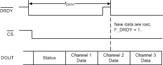
DRDY indicates when a new conversion result is ready for retrieval. When DRDY transitions from high to low, new conversion data are ready. The DRDY signal remains low for the duration of the data frame and returns high either when CS returns high (signaling the completion of the frame), or prior to new data being available. The high-to-low DRDY transition occurs at the set data rate regardless of the CS state. If data are not completely shifted out when new data are ready, the DRDY signal toggles high for a duration of 0.5 × tMOD and back low. The device sets the F_DRDY bit in the STAT_1 register indicating that the DOUT output shift register is not updated with the new conversion result. Figure 61 shows an example of new data being ready before previous data are shifted out, causing the new conversion result to be lost. The DRDY pin is always actively driven, even when CS is high.
ADS131A02 ADS131A04 DRDYduringreadback_Asynchronous_sbas590.gifFigure 61. Asynchronous Interrupt Mode Conversion Update During a Read Operation