SBAS590E March 2016 – June 2020 ADS131A02 , ADS131A04
PRODUCTION DATA.
- 1 Features
- 2 Applications
- 3 Description
- 4 Revision History
- 5 Device Comparison Table
- 6 Pin Configuration and Functions
-
7 Specifications
- 7.1 Absolute Maximum Ratings
- 7.2 ESD Ratings
- 7.3 Recommended Operating Conditions
- 7.4 Thermal Information
- 7.5 Electrical Characteristics
- 7.6 Timing Requirements: Asynchronous Interrupt Interface Mode
- 7.7 Switching Characteristics: Asynchronous Interrupt Interface Mode
- 7.8 Timing Requirements: Synchronous Master Interface Mode
- 7.9 Switching Characteristics: Synchronous Master Interface Mode
- 7.10 Timing Requirements: Synchronous Slave Interface Mode
- 7.11 Switching Characteristics: Synchronous Slave Interface Mode
- 7.12 Typical Characteristics
- 8 Parameter Measurement Information
-
9 Detailed Description
- 9.1 Overview
- 9.2 Functional Block Diagram
- 9.3 Feature Description
- 9.4 Device Functional Modes
- 9.5
Programming
- 9.5.1 Interface Protocol
- 9.5.2 SPI Interface
- 9.5.3
SPI Command Definitions
- 9.5.3.1 NULL: Null Command
- 9.5.3.2 RESET: Reset to POR Values
- 9.5.3.3 STANDBY: Enter Standby Mode
- 9.5.3.4 WAKEUP: Exit Standby Mode
- 9.5.3.5 LOCK: Lock ADC Registers
- 9.5.3.6 UNLOCK: Unlock ADC Registers
- 9.5.3.7 RREG: Read a Single Register
- 9.5.3.8 RREGS: Read Multiple Registers
- 9.5.3.9 WREG: Write Single Register
- 9.5.3.10 WREGS: Write Multiple Registers
- 9.6
Register Maps
- 9.6.1
User Register Description
- 9.6.1.1 ID_MSB: ID Control Register MSB (address = 00h) [reset = xxh]
- 9.6.1.2 ID_LSB: ID Control Register LSB (address = 01h) [reset = xxh]
- 9.6.1.3 STAT_1: Status 1 Register (address = 02h) [reset = 00h]
- 9.6.1.4 STAT_P: Positive Input Fault Detect Status Register (address = 03h) [reset = 00h]
- 9.6.1.5 STAT_N: Negative Input Fault Detect Status Register (address = 04h) [reset = 00h]
- 9.6.1.6 STAT_S: SPI Status Register (address = 05h) [reset = 00h]
- 9.6.1.7 ERROR_CNT: Error Count Register (address = 06h) [reset = 00h]
- 9.6.1.8 STAT_M2: Hardware Mode Pin Status Register (address = 07h) [reset = xxh]
- 9.6.1.9 Reserved Registers (address = 08h to 0Ah) [reset = 00h]
- 9.6.1.10 A_SYS_CFG: Analog System Configuration Register (address = 0Bh) [reset = 60h]
- 9.6.1.11 D_SYS_CFG: Digital System Configuration Register (address = 0Ch) [reset = 3Ch]
- 9.6.1.12 CLK1: Clock Configuration 1 Register (address = 0Dh) [reset = 08h]
- 9.6.1.13 CLK2: Clock Configuration 2 Register (address = 0Eh) [reset = 86h]
- 9.6.1.14 ADC_ENA: ADC Channel Enable Register (address = 0Fh) [reset = 00h]
- 9.6.1.15 Reserved Register (address = 10h) [reset = 00h]
- 9.6.2 ADCx: ADC Channel Digital Gain Configuration Registers (address = 11h to 14h) [reset = 00h]
- 9.6.1
User Register Description
- 10Application and Implementation
- 11Power Supply Recommendations
- 12Layout
- 13Device and Documentation Support
- 14Mechanical, Packaging, and Orderable Information
Package Options
Refer to the PDF data sheet for device specific package drawings
Mechanical Data (Package|Pins)
- PBS|32
Thermal pad, mechanical data (Package|Pins)
- PBS|32
Orderable Information
9.3.6 Digital Decimation Filter
The digital filter receives the modulator output and decimates the data stream to create the final conversion result. The digital filter on each channel consists of a third-order sinc filter. The oversampling ratio (OSR) determines the number of samples taken to create the output data word, and is set by the modulator rate divided by the data rate (fMOD / fDATA). The OSR of the sinc filters is adjusted by the OSR[3:0] bits in the CLK2 register. The OSR setting is a global setting that affects all channels and, therefore, all channels operate at the same data rate in the device. By adjusting the OSR, tradeoffs can be made between noise and data rate to optimize the signal chain: filter more for lower noise (thus creating lower data rates), filter less for higher data rates.
The sinc filter is a variable decimation rate, third-order, low-pass filter. Data are supplied to this section of the filter from the modulator at the rate of fMOD. Equation 6 shows the scaled sinc3 filter Z-domain transfer function. As shown in Table 6, the integer N is the set OSR and the integer K is a scaling factor for OSR values that are not an integer power of 2.

Equation 7 shows the sinc filter frequency domain transfer function. As shown in Table 6, the integer N is the set OSR and the integer K is a scaling factor for OSR values that are not an integer power of 2.

where
Table 6. K Scaling Factor
| OSR (N) | K SCALING VALUE |
|---|---|
| 800, 400, 200 | 0.9983778 |
| 4096, 2048, 1024, 512, 256, 128, 64, 32 | 1.0 |
| 768, 384, 192, 96, 48 | 1.00195313 |
The sinc3 filter has notches (or zeroes) that occur at the output data rate and multiples thereof. At these frequencies, the filter has infinite attenuation. Figure 45 and Figure 46 illustrate the digital filter frequency response out to a normalized input frequency (fIN / fDATA) of 5 and 0.5, respectively. Figure 47, Figure 48, and Figure 49 illustrate the frequency response for OSR = 32, OSR = 512, and OSR = 4096 up to fMOD, respectively.
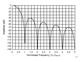 Figure 45. Sinc3 Filter Frequency Response
 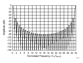 Figure 47. Sinc3 Filter Frequency Response (OSR 32)
 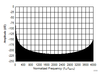 Figure 49. Sinc3 Filter Frequency Response (OSR 4096)
 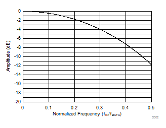 Figure 46. Sinc3 Filter Roll-Off
 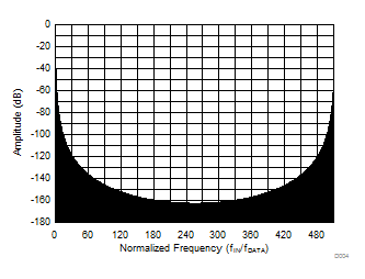 Figure 48. Sinc3 Filter Frequency Response (OSR 512)
 The K scaling factor for OSR values that are not an integer power of two adds a non-integer gain factor to the sinc3 frequency response across all frequencies. The host must account for the K scaling factor to obtain the ADC gain error given in the Electrical Characteristics table. Figure 50 overlays the digital filter frequency response for the three K scaling options in Table 6. Graph scaling is set to a narrow limit to show the small gain variation between OSR values.
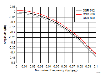 Figure 50. Non-Binary OSR Sinc3 Filter Frequency Response
 The ADS131A0x immediately begins ADC conversions when powered up and brought out of standby mode using the WAKEUP command. The DRDY falling edge indicates when each ADC conversion completes. The sinc3 digital filter requires three conversion cycles to settle (tSETTLE), assuming the analog input has settled to its final value. The output data are not gated when the digital filter settles, meaning that the first two ADC conversion results show unsettled data from the filter path before settled data are available for the third ADC conversion. The first two unsettled ADC conversions, though unsettled, can be used for diagnostic purposes to ensure the ADC is coming out of standby as expected.
In addition to the sinc3 filter settling, the ADC requires an extra data period to report the conversion data. After the ADC accumulates the digital filter data, an additional data period is required for the ADC data to reach the DOUT buffer. Because of the digital filter settling and the DOUT buffer, the device requires four data periods to retrieve data from DOUT. Figure 51 shows the data ready behavior and time needed for the digital filter settling and data retrieval coming out of standby.
 Figure 51. Sinc3 Filter Settling
 The digital filter uses a multiple stage linear-phase digital filter. Linear-phase filters exhibit constant delay time across all input frequencies (also known as constant group delay). This behavior results in zero-phase error when measuring multi-tone signals. For more information about group delay in delta-sigma ADCs, see the Accounting for delay from multiple sources in delta-sigma ADCs white paper.