SBAS520C February 2011 – June 2017 ADS4122 , ADS4125 , ADS4142 , ADS4145
PRODUCTION DATA.
- 1 Features
- 2 Applications
- 3 Description
- 4 Revision History
- 5 Device Family Comparison
- 6 Pin Configuration and Functions
-
7 Specifications
- 7.1 Absolute Maximum Ratings
- 7.2 ESD Ratings
- 7.3 Recommended Operating Conditions
- 7.4 Thermal Information
- 7.5 Electrical Characteristics: ADS412x
- 7.6 Electrical Characteristics: ADS414x
- 7.7 Electrical Characteristics: General
- 7.8 Digital Characteristics
- 7.9 Timing Requirements: LVDS and CMOS Modes
- 7.10 Serial Interface Timing Characteristics
- 7.11 Reset Timing Requirements
- 7.12 Timing Characteristics at Lower Sampling Frequencies
- 7.13 Typical Characteristics: ADS4122
- 7.14 Typical Characteristics: ADS4125
- 7.15 Typical Characteristics: ADS4142
- 7.16 Typical Characteristics: ADS4145
- 7.17 Typical Characteristics: Common
- 7.18 Typical Characteristics: Contour
- 8 Detailed Description
- 9 Application and Implementation
- 10Power Supply Recommendations
- 11Layout
- 12Device and Documentation Support
- 13Mechanical, Packaging, and Orderable Information
Package Options
Mechanical Data (Package|Pins)
- RGZ|48
Thermal pad, mechanical data (Package|Pins)
- RGZ|48
Orderable Information
1 Features
- Ultra-Low Power With 1.8-V Single Supply:
- 103-mW Total Power at 65 MSPS
- 153-mW Total Power at 125 MSPS
- High Dynamic Performance:
- SNR: 72.2 dBFS at 170 MHz
- SFDR: 81 dBc at 170 MHz
- Dynamic Power Scaling With Sample Rate
- Idle Channel SNR 74.8 dBFS (ADS414x)
- Output Interface:
- Double Data Rate (DDR) LVDS With Programmable Swing and Strength:
- Standard Swing: 350 mV
- Low Swing: 200 mV
- Default Strength: 100-Ω Termination
- 2x Strength: 50-Ω Termination
- 1.8-V Parallel CMOS Interface Also Supported
- Double Data Rate (DDR) LVDS With Programmable Swing and Strength:
- Programmable Gain up to 6 dB for SNR, SFDR Trade-Off
- DC Offset Correction
- Supports Low Input Clock Amplitude Down to 200 mVPP
2 Applications
3 Description
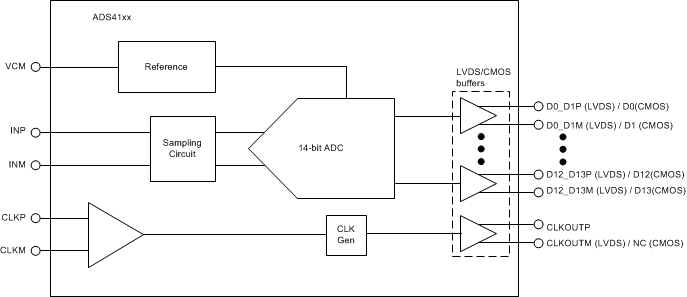
The ADS412x and ADS414x devices are lower-sampling speed variants in the ADS41xx family of analog-to-digital converters (ADCs). These devices use innovative design techniques to achieve high dynamic performance, while consuming extremely low power at 1.8-V supply. The devices are well-suited for multi-carrier, wide bandwidth communications applications.
The ADS412x and ADS414x devices have fine gain options that can be used to improve SFDR performance at lower full-scale input ranges, especially at high input frequencies. They include a dc offset correction loop that can be used to cancel the ADC offset. At lower sampling rates, the ADC automatically operates at scaled down power with no loss in performance.
The ADS412x and ADS414x devices are available in a compact VQFN-48 package and are specified over the industrial temperature range (–40°C to +85°C).
Device Information(1)
| PART NUMBER | PACKAGE | BODY SIZE (NOM) |
|---|---|---|
| ADS4122 | VQFN (48) | 7.00 mm × 7.00 mm |
| ADS4125 | ||
| ADS4142 | ||
| ADS4145 |
- For all available packages, see the orderable addendum at the end of the data sheet.
