SBAS533E March 2011 – February 2023 ADS4222 , ADS4225 , ADS4226 , ADS4242 , ADS4245 , ADS4246
PRODUCTION DATA
- 1 Features
- 2 Applications
- 3 Description
- 4 Revision History
- 5 Description (continued)
- 6 Pin Configuration and Functions
-
7 Specifications
- 7.1 Absolute Maximum Ratings
- 7.2 ESD Ratings
- 7.3 Recommended Operating Conditions
- 7.4 Thermal Information
- 7.5 Electrical Characteristics: ADS4246, ADS4245, ADS4242
- 7.6 Electrical Characteristics: ADS4226, ADS4225, ADS4222
- 7.7 Electrical Characteristics: General
- 7.8 Digital Characteristics
- 7.9 Timing Requirements: LVDS and CMOS Modes (1)
- 7.10 Serial Interface Timing Characteristics (1)
- 7.11 Reset Timing (Only When Serial Interface Is Used)
- 7.12 Typical Characteristics
-
8 Detailed Description
- 8.1 Overview
- 8.2 Functional Block Diagrams
- 8.3 Feature Description
- 8.4 Device Functional Modes
- 8.5 Programming
- 8.6 Register Maps
- 9 Application and Implementation
- 10Device and Documentation Support
- 11Mechanical, Packaging, and Orderable Information
Package Options
Mechanical Data (Package|Pins)
- RGC|64
Thermal pad, mechanical data (Package|Pins)
- RGC|64
Orderable Information
8.3.1.1 Drive Circuit Requirements
For optimum performance, the analog inputs must be driven differentially. This operation improves the common-mode noise immunity and even-order harmonic rejection. A 5Ω to 15Ω resistor in series with each input pin is recommended to damp out ringing caused by package parasitics.
SFDR performance can be limited as a result of several reasons, including the effects of sampling glitches, nonlinearity of the sampling circuit, and nonlinearity of the quantizer that follows the sampling circuit. Depending on the input frequency, sample rate, and input amplitude, one of these factors plays a dominant part in limiting performance. At very high input frequencies (greater than approximately 300 MHz), SFDR is determined largely by the device sampling circuit nonlinearity. At low input amplitudes, the quantizer nonlinearity usually limits performance.
Glitches are caused by the opening and closing of the sampling switches. The driving circuit should present a low source impedance to absorb these glitches. Otherwise, glitches could limit performance, primarily at low input frequencies (up to approximately 200 MHz). It is also necessary to present low impedance (less than 50Ω) for the common-mode switching currents. This configuration can be achieved by using two resistors from each input terminated to the common-mode voltage (VCM).
The device includes an internal R-C filter from each input to ground. The purpose of this filter is to absorb the sampling glitches inside the device itself. The cutoff frequency of the R-C filter involves a trade-off. A lower cutoff frequency (larger C) absorbs glitches better, but it reduces the input bandwidth. On the other hand, with a higher cutoff frequency (smaller C), bandwidth support is maximized. However, the sampling glitches now must be supplied by the external drive circuit. This tradeoff has limitations as a result of the presence of the package bond-wire inductance.
In the ADS424x/422x, the R-C component values have been optimized while supporting high input bandwidth (up to 550 MHz). However, in applications with input frequencies up to 200 MHz to 300 MHz, the filtering of the glitches can be improved further using an external R-C-R filter; see GUID-A46F7AA7-980B-49F9-9092-6B1E819DC75A.html#SBAS483IMG9467 and GUID-A46F7AA7-980B-49F9-9092-6B1E819DC75A.html#SBAS483IMG5556.
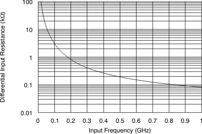
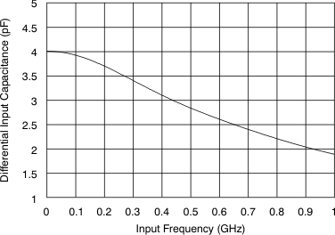
In addition, the drive circuit may have to be designed to provide a low insertion loss over the desired frequency range and matched impedance to the source. Furthermore, the ADC input impedance must be considered. #SBAS483IMG6440 and #SBAS483IMG3505 show the impedance (ZIN = RIN || CIN) looking into the ADC input pins.
 Figure 8-4 ADC Analog Input Resistance (RIN) Across Frequency
 Figure 8-5 ADC Analog Input Capacitance (CIN) Across Frequency