SBAS533E March   2011  – February 2023 ADS4222 , ADS4225 , ADS4226 , ADS4242 , ADS4245 , ADS4246

PRODUCTION DATA  

  1. Features
  2. Applications
  3. Description
  4. Revision History
  5. Description (continued)
  6. Pin Configuration and Functions
    1.     Pin Functions – LVDS Mode
    2.     Pin Functions – CMOS Mode
  7. Specifications
    1. 7.1  Absolute Maximum Ratings
    2. 7.2  ESD Ratings
    3. 7.3  Recommended Operating Conditions
    4. 7.4  Thermal Information
    5. 7.5  Electrical Characteristics: ADS4246, ADS4245, ADS4242
    6. 7.6  Electrical Characteristics: ADS4226, ADS4225, ADS4222
    7. 7.7  Electrical Characteristics: General
    8. 7.8  Digital Characteristics
    9. 7.9  Timing Requirements: LVDS and CMOS Modes (1)
    10. 7.10 Serial Interface Timing Characteristics (1)
    11. 7.11 Reset Timing (Only When Serial Interface Is Used)
    12. 7.12 Typical Characteristics
      1. 7.12.1 ADS4246
      2. 7.12.2 ADS4245
      3. 7.12.3 ADS4242
      4. 7.12.4 ADS4226
      5. 7.12.5 ADS4225
      6. 7.12.6 ADS4222
      7. 7.12.7 General
      8. 7.12.8 Contour
  8. Detailed Description
    1. 8.1 Overview
    2. 8.2 Functional Block Diagrams
    3. 8.3 Feature Description
      1. 8.3.1 Analog Input
        1. 8.3.1.1 Drive Circuit Requirements
        2. 8.3.1.2 Driving Circuit
      2. 8.3.2 Clock Input
      3. 8.3.3 Digital Functions
      4. 8.3.4 Gain for SFDR/SNR Trade-off
      5. 8.3.5 Offset Correction
    4. 8.4 Device Functional Modes
      1. 8.4.1 Power-Down
        1. 8.4.1.1 Global Power-Down
        2. 8.4.1.2 Channel Standby
        3. 8.4.1.3 Input Clock Stop
    5. 8.5 Programming
      1. 8.5.1 47
      2. 8.5.2 Parallel Configuration Only
      3. 8.5.3 Serial Interface Configuration Only
      4. 8.5.4 Using Both Serial Interface and Parallel Controls
      5. 8.5.5 Parallel Configuration Details
      6. 8.5.6 Serial Interface Details
        1. 8.5.6.1 Register Initialization
        2. 8.5.6.2 Serial Register Readout
      7. 8.5.7 Digital Output Information
        1. 8.5.7.1 Output Interface
        2. 8.5.7.2 DDR LVDS Outputs
        3. 8.5.7.3 LVDS Buffer
        4. 8.5.7.4 Parallel CMOS Interface
        5. 8.5.7.5 CMOS Interface Power Dissipation
        6. 8.5.7.6 Multiplexed Mode of Operation
        7. 8.5.7.7 Output Data Format
    6. 8.6 Register Maps
      1. 8.6.1 64
      2. 8.6.2 Description Of Serial Registers
  9. Application and Implementation
    1. 9.1 Application Information
    2. 9.2 Typical Application
      1. 9.2.1 Design Requirements
      2. 9.2.2 Detailed Design Procedure
        1. 9.2.2.1 Analog Input
        2. 9.2.2.2 Clock Driver
        3. 9.2.2.3 Digital Interface
        4. 9.2.2.4 SNR and Clock Jitter
      3. 9.2.3 Application Curves
    3. 9.3 Power Supply Recommendations
      1. 9.3.1 Sharing DRVDD and AVDD Supplies
      2. 9.3.2 Using DC/DC Power Supplies
      3. 9.3.3 Power Supply Bypassing
    4. 9.4 Layout
      1. 9.4.1 Layout Guidelines
        1. 9.4.1.1 Grounding
        2. 9.4.1.2 Supply Decoupling
        3. 9.4.1.3 Exposed Pad
        4. 9.4.1.4 Routing Analog Inputs
      2. 9.4.2 Layout Example
  10. 10Device and Documentation Support
    1. 10.1 Device Support
      1. 10.1.1 Device Nomenclature
    2. 10.2 Documentation Support
      1. 10.2.1 Related Documentation
    3. 10.3 Support Resources
    4. 10.4 Trademarks
    5. 10.5 Electrostatic Discharge Caution
    6. 10.6 Glossary
  11. 11Mechanical, Packaging, and Orderable Information

Package Options

Mechanical Data (Package|Pins)
Thermal pad, mechanical data (Package|Pins)
Orderable Information

Serial Register Readout

The device includes a mode where the contents of the internal registers can be read back. This readback mode may be useful as a diagnostic check to verify the serial interface communication between the external controller and the ADC. To use readback mode, follow this procedure:

  1. Set the READOUT register bit to 1. This setting disables any further writes to the registers.
  2. Initiate a serial interface cycle specifying the address of the register (A7 to A0) whose content has to be read.
  3. The device outputs the contents (D7 to D0) of the selected register on the SDOUT pin (pin 64).
  4. The external controller can latch the contents at the SCLK falling edge.
  5. To enable register writes, reset the READOUT register bit to 0.

The serial register readout works with both CMOS and LVDS interfaces on pin 64.

When READOUT is disabled, the SDOUT pin is in high-impedance state. If serial readout is not used, the SDOUT pin must float.
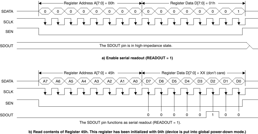
GUID-1CF35332-2106-444F-B96F-8672CB242248-low.gifFigure 8-18 Serial Readout Timing Diagram
GUID-02F31983-23B2-466D-9DB6-387B0AC0461B-low.gif
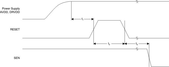
A high pulse on the RESET pin is required in the serial interface mode when initialized through a hardware reset. For parallel interface operation, RESET must be permanently tied high.
Figure 8-19 Reset Timing Diagram