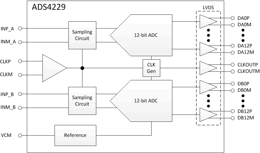
The ADS4229 is a member of the ADS42xx ultralow-power family of dual-channel, 12-bit and 14-bit analog-to-digital converters (ADCs). Innovative design techniques are used to achieve high dynamic performance, while consuming extremely low power with a 1.8-V supply. This topology makes the ADS4229 well-suited for multi-carrier, wide-bandwidth communications applications.
The ADS4229 has gain options that can be used to improve spurious-free dynamic range (SFDR) performance at lower full-scale input ranges. This device also includes a dc offset correction loop that can be used to cancel the ADC offset. Both double data rate (DDR) low-voltage differential signaling (LVDS) and parallel complementary metal oxide semiconductor (CMOS) digital output interfaces are available in a compact QFN-64 PowerPAD™ package.
The device includes internal references while the traditional reference pins and associated decoupling capacitors have been eliminated. The ADS4229 is specified over the industrial temperature range (–40°C to +85°C).
PART NUMBER | PACKAGE | BODY SIZE (NOM) |
---|---|---|
ADS4229 | VQFN (64) | 9.00 mm × 9.00 mm |
Changes from B Revision (August 2012) to C Revision
Changes from A Revision (October 2011) to B Revision
Changes from * Revision (June 2011) to A Revision
The ADS4229 is pin-compatible with the previous generation ADS62P49 data converter; this similar architecture enables easy migration. However, there are some important differences between the two device generations, summarized in Table 1.
PIN | I/O | DESCRIPTION | |
---|---|---|---|
NAME | NO. | ||
AGND | 17 | I | Analog ground |
18 | |||
21 | |||
24 | |||
27 | |||
28 | |||
31 | |||
32 | |||
AVDD | 16 | I | Analog power supply |
22 | |||
23 | |||
34 | |||
CLKM | 26 | I | Differential clock negative input |
CLKP | 25 | I | Differential clock positive input |
CTRL1 | 35 | I | Digital control input pins. Together, they control the various power-down modes. |
CTRL2 | 36 | I | Digital control input pins. Together, they control the various power-down modes. |
CTRL3 | 37 | I | Digital control input pins. Together, they control the various power-down modes. |
CLKOUTP | 57 | O | Differential output clock, true |
CLKOUTM | 56 | O | Differential output clock, complement |
DA0M | 42 | O | Channel A differential output data pair, D0 and D1 multiplexed |
DA0P | 43 | ||
DA2M | 44 | O | Channel A differential output data D2 and D3 multiplexed |
DA2P | 45 | ||
DA4M | 46 | O | Channel A differential output data D4 and D5 multiplexed |
DA4P | 47 | ||
DA6M | 50 | O | Channel A differential output data D6 and D7 multiplexed |
DA6P | 51 | ||
DA8M | 52 | O | Channel A differential output data D8 and D9 multiplexed |
DA8P | 53 | ||
DA10M | 54 | O | Channel A differential output data D10 and D11 multiplexed |
DA10P | 55 | ||
DB0M | 62 | O | Channel B differential output data pair, D0 and D1 multiplexed |
DB0P | 63 | ||
DB2M | 2 | O | Channel B differential output data D2 and D3 multiplexed |
DB2P | 3 | ||
DB4M | 4 | O | Channel B differential output data D4 and D5 multiplexed |
DB4P | 5 | ||
DB6M | 6 | O | Channel B differential output data D6 and D7 multiplexed |
DB6P | 7 | ||
DB8M | 8 | O | Channel B differential output data D8 and D9 multiplexed |
DB8P | 9 | ||
DB10M | 10 | O | Channel B differential output data D10 and D11 multiplexed |
DB10P | 11 | ||
DRGND | 49 | I | Output buffer ground |
PAD | |||
DRVDD | 1 | I | Output buffer supply |
48 | |||
INP_A | 29 | I | Differential analog positive input, channel A |
INM_A | 30 | I | Differential analog negative input, channel A |
INP_B | 19 | I | Differential analog positive input, channel B |
INM_B | 20 | I | Differential analog negative input, channel B |
NC | 38 | — | Do not connect, must be floated |
39 | |||
40 | |||
41 | |||
58 | |||
59 | |||
60 | |||
61 | |||
RESET | 12 | I | Serial interface RESET input. When using the serial interface mode, the internal registers must be initialized through a hardware RESET by applying a high pulse on this pin or by using the software reset option; refer to the Serial Interface Configuration section. In parallel interface mode, the RESET pin must be permanently tied high. SCLK and SEN are used as parallel control pins in this mode. This pin has an internal 150-kΩ pull-down resistor. |
SCLK | 13 | I | This pin functions as a serial interface clock input when RESET is low. It controls the low-speed mode selection when RESET is tied high; see Table 7 for detailed information. This pin has an internal 150-kΩ pull-down resistor. |
SDATA | 14 | I | Serial interface data input; this pin has an internal 150-kΩ pull-down resistor. |
SDOUT | 64 | O | This pin functions as a serial interface register readout when the READOUT bit is enabled. When READOUT = 0, this pin is put into a high-impedance state. |
VCM | 23 | O | This pin outputs the common-mode voltage (0.95 V) that can be used externally to bias the analog input pins |
PIN | I/O | DESCRIPTION | |
---|---|---|---|
NAME | NO. | ||
AGND | 17 | I | Analog ground |
18 | |||
21 | |||
24 | |||
27 | |||
28 | |||
31 | |||
32 | |||
AVDD | 16 | I | Analog power supply |
22 | |||
33 | |||
34 | |||
CLKM | 26 | I | Differential clock negative input |
CLKOUT | 57 | O | CMOS output clock |
CLKP | 25 | I | Differential clock positive input |
CTRL1 | 35 | I | Digital control input pins. Together, they control various power-down modes. |
CTRL2 | 36 | I | Digital control input pins. Together, they control various power-down modes. |
CTRL3 | 37 | I | Digital control input pins. Together, they control various power-down modes. |
DA0 | 42 | O | Channel A ADC output data bits, CMOS levels |
DA1 | 43 | ||
DA2 | 44 | ||
DA3 | 45 | ||
DA4 | 46 | ||
DA5 | 47 | ||
DA6 | 50 | ||
DA7 | 51 | ||
DA8 | 52 | ||
DA9 | 53 | ||
DA10 | 54 | ||
DA11 | 55 | ||
DB0 | 62 | O | Channel B ADC output data bits, CMOS levels |
DB1 | 63 | ||
DB2 | 2 | ||
DB3 | 3 | ||
DB4 | 4 | ||
DB5 | 5 | ||
DB6 | 6 | ||
DB7 | 7 | ||
DB8 | 8 | ||
DB9 | 9 | ||
DB10 | 10 | ||
DB11 | 11 | ||
DRGND | 49 | I | Output buffer ground |
PAD | |||
DRVDD | 1 | I | Output buffer supply |
48 | |||
NC | — | — | Do not connect, must be floated |
RESET | 12 | I | Serial interface RESET input. When using the serial interface mode, the internal registers must be initialized through a hardware RESET by applying a high pulse on this pin or by using the software reset option; refer to the Serial Interface Configuration section. In parallel interface mode, the RESET pin must be permanently tied high. SDATA and SEN are used as parallel control pins in this mode. This pin has an internal 150-kΩ pull-down resistor. |
INM_A | 30 | I | Differential analog negative input, channel A |
INP_A | 29 | I | Differential analog positive input, channel A |
INM_B | 20 | I | Differential analog negative input, channel B |
INP_B | 19 | I | Differential analog positive input, channel B |
SCLK | 13 | I | This pin functions as a serial interface clock input when RESET is low. It controls the low-speed mode when RESET is tied high; see Table 7 for detailed information. This pin has an internal 150-kΩ pull-down resistor. |
SDATA | 14 | I | Serial interface data input; this pin has an internal 150-kΩ pull-down resistor. |
SDOUT | 64 | O | This pin functions as a serial interface register readout when the READOUT bit is enabled. When READOUT = 0, this pin is put into a high-impedance state. |
SEN | 15 | I | This pin functions as a serial interface enable input when RESET is low. It controls the output interface and data format selection when RESET is tied high; see Table 8 for detailed information. This pin has an internal 150-kΩ pull-up resistor to AVDD. |
VCM | 23 | O | This pin outputs the common-mode voltage (0.95 V) that can be used externally to bias the analog input pins |
UNUSED | 56 | — | This pin is not used in the CMOS interface |
MIN | MAX | UNIT | ||
---|---|---|---|---|
Supply voltage, AVDD | –0.3 | 2.1 | V | |
Supply voltage, DRVDD | –0.3 | 2.1 | V | |
Voltage between AGND and DRGND | –0.3 | 0.3 | V | |
Voltage between AVDD to DRVDD (when AVDD leads DRVDD) | –2.4 | 2.4 | V | |
Voltage between DRVDD to AVDD (when DRVDD leads AVDD) | –2.4 | 2.4 | V | |
Voltage applied to input pins | INP_A, INM_A, INP_B, INM_B | –0.3 | Minimum (1.9, AVDD + 0.3) |
V |
CLKP, CLKM(2) | –0.3 | AVDD + 0.3 | V | |
RESET, SCLK, SDATA, SEN, CTRL1, CTRL2, CTRL3 |
–0.3 | 3.9 | V | |
Operating free-air temperature, TA | –40 | 85 | °C | |
Operating junction temperature, TJ | 125 | °C | ||
Storage temperature, Tstg | –65 | 150 | °C |
VALUE | UNIT | |||
---|---|---|---|---|
V(ESD) | Electrostatic discharge | Human body model (HBM), per ANSI/ESDA/JEDEC JS-001(1) | 2000 | V |
MIN | NOM | MAX | UNIT | ||
---|---|---|---|---|---|
SUPPLIES | |||||
Analog supply voltage, AVDD | 1.7 | 1.8 | 1.9 | V | |
Digital supply voltage, DRVDD | 1.7 | 1.8 | 1.9 | V | |
ANALOG INPUTS | |||||
Differential input voltage range | 2 | VPP | |||
Input common-mode voltage | VCM ± 0.05 | V | |||
Maximum analog input frequency with 2-VPP input amplitude(1) | 400 | MHz | |||
Maximum analog input frequency with 1-VPP input amplitude(1) | 600 | MHz | |||
CLOCK INPUT | |||||
Input clock sample rate | |||||
Low-speed mode enabled(2) | 1 | 80 | MSPS | ||
Low-speed mode disabled(2) (by default after reset) | 80 | 250 | MSPS | ||
Input clock amplitude differential (VCLKP – VCLKM) |
Sine wave, ac-coupled | 0.2 | 1.5 | VPP | |
LVPECL, ac-coupled | 1.6 | VPP | |||
LVDS, ac-coupled | 0.7 | VPP | |||
LVCMOS, single-ended, ac-coupled | 1.5 | V | |||
Input clock duty cycle | |||||
Low-speed mode disabled | 35% | 50% | 65% | ||
Low-speed mode enabled | 40% | 50% | 60% | ||
DIGITAL OUTPUTS | |||||
Maximum external load capacitance from each output pin to DRGND, CLOAD | 5 | pF | |||
Differential load resistance between the LVDS output pairs (LVDS mode), RLOAD | 100 | Ω | |||
Operating free-air temperature, TA | –40 | +85 | °C |
THERMAL METRIC(1) | ADS4229 | UNIT | |
---|---|---|---|
RGC (VQFN) | |||
64 PINS | |||
RθJA | Junction-to-ambient thermal resistance | 23.9 | °C/W |
RθJC(top) | Junction-to-case (top) thermal resistance | 10.9 | °C/W |
RθJB | Junction-to-board thermal resistance | 4.3 | °C/W |
ψJT | Junction-to-top characterization parameter | 0.1 | °C/W |
ψJB | Junction-to-board characterization parameter | 4.4 | °C/W |
RθJC(bot) | Junction-to-case (bottom) thermal resistance | 0.6 | °C/W |
PARAMETER | MIN | TYP | MAX | UNIT | |
---|---|---|---|---|---|
ANALOG INPUTS | |||||
Differential input voltage range | 2 | VPP | |||
Differential input resistance (at 200 MHz) | 0.75 | kΩ | |||
Differential input capacitance (at 200 MHz) | 3.7 | pF | |||
Analog input bandwidth (with 50-Ω source impedance, and 50-Ω termination) |
550 | MHz | |||
Analog input common-mode current (per input pin of each channel) |
1.5 | µA/MSPS | |||
Common-mode output voltage | VCM | 0.95(2) | V | ||
VCM output current capability | 4 | mA | |||
DC ACCURACY | |||||
Offset error | –15 | 2.5 | 15 | mV | |
Temperature coefficient of offset error | 0.003 | mV/°C | |||
Gain error as a result of internal reference inaccuracy alone | EGREF | –2 | 2 | %FS | |
Gain error of channel alone | EGCHAN | ±0.1 | 1 | %FS | |
Temperature coefficient of EGCHAN | 0.002 | Δ%/°C | |||
POWER SUPPLY | |||||
IAVDD Analog supply current |
167 | 190 | mA | ||
IDRVDD Output buffer supply current LVDS interface, 350-mV swing with 100-Ω external termination, fIN = 2.5 MHz |
136 | 160 | mA | ||
IDRVDD Output buffer supply current CMOS interface, no load capacitance, fIN = 2.5 MHz(1) |
94 | mA | |||
Analog power | 301 | mW | |||
Digital power LVDS interface, 350-mV swing with 100-Ω external termination, fIN = 2.5 MHz |
245 | mW | |||
Digital power CMOS interface, 8-pF external load capacitance(1) fIN = 2.5 MHz |
169 | mW | |||
Global power-down | 25 | mW |
PARAMETER | TEST CONDITIONS | MIN | TYP | MAX | UNIT | |
---|---|---|---|---|---|---|
DIGITAL INPUTS (RESET, SCLK, SDATA, SEN, CTRL1, CTRL2, CTRL3)(1) | ||||||
High-level input voltage | All digital inputs support 1.8-V and 3.3-V CMOS logic levels | 1.3 | V | |||
Low-level input voltage | 0.4 | V | ||||
High-level input current | SDATA, SCLK(2) | VHIGH = 1.8 V | 10 | µA | ||
SEN(3) | VHIGH = 1.8 V | 0 | µA | |||
Low-level input current | SDATA, SCLK | VLOW = 0 V | 0 | µA | ||
SEN | VLOW = 0 V | 10 | µA | |||
DIGITAL OUTPUTS, CMOS INTERFACE (DA[13:0], DB[13:0], CLKOUT, SDOUT) | ||||||
High-level output voltage | DRVDD – 0.1 | DRVDD | V | |||
Low-level output voltage | 0 | 0.1 | V | |||
Output capacitance (internal to device) | pF | |||||
DIGITAL OUTPUTS, LVDS INTERFACE | ||||||
High-level output differential voltage |
VODH | With an external 100-Ω termination |
270 | 350 | 430 | mV |
Low-level output differential voltage |
VODL | With an external 100-Ω termination |
–430 | –350 | –270 | mV |
Output common-mode voltage | VOCM | 0.9 | 1.05 | 1.25 | V |
PARAMETER | DESCRIPTION | MIN | TYP | MAX | UNIT | |
---|---|---|---|---|---|---|
tA | Aperture delay | 0.5 | 0.8 | 1.1 | ns | |
Aperture delay matching | Between the two channels of the same device | ±70 | ps | |||
Variation of aperture delay | Between two devices at the same temperature and DRVDD supply | ±150 | ps | |||
tJ | Aperture jitter | 140 | fS rms | |||
Wakeup time | Time to valid data after coming out of STANDBY mode | 50 | 100 | µs | ||
Time to valid data after coming out of GLOBAL power-down mode | 100 | 500 | µs | |||
ADC latency(4) | Default latency after reset | 16 | Clock cycles | |||
Digital functions enabled (EN DIGITAL = 1) | 24 | Clock cycles | ||||
DDR LVDS MODE(2) | ||||||
tSU | Data setup time | Data valid(3) to zero-crossing of CLKOUTP | 0.6 | 0.88 | ns | |
tH | Data hold time | Zero-crossing of CLKOUTP to data becoming invalid(3) | 0.33 | 0.55 | ns | |
tPDI | Clock propagation delay | Input clock rising edge cross-over to output clock rising edge cross-over | 5 | 6 | 7.5 | ns |
LVDS bit clock duty cycle | Duty cycle of differential clock, (CLKOUTP-CLKOUTM) | 48% | ||||
tRISE, tFALL |
Data rise time, Data fall time |
Rise time measured from –100 mV to +100 mV Fall time measured from +100 mV to –100 mV 1 MSPS ≤ Sampling frequency ≤ 250 MSPS |
0.13 | ns | ||
tCLKRISE, tCLKFALL |
Output clock rise time, Output clock fall time |
Rise time measured from –100 mV to +100 mV Fall time measured from +100 mV to –100 mV 1 MSPS ≤ Sampling frequency ≤ 250 MSPS |
0.13 | ns | ||
PARALLEL CMOS MODE | ||||||
tPDI | Clock propagation delay | Input clock rising edge cross-over to output clock rising edge cross-over | 4.5 | 6.2 | 8.5 | ns |
Output clock duty cycle | Duty cycle of output clock, CLKOUT 1 MSPS ≤ Sampling frequency ≤ 200 MSPS |
50% | ||||
tRISE, tFALL |
Data rise time, Data fall time |
Rise time measured from 20% to 80% of DRVDD Fall time measured from 80% to 20% of DRVDD 1 MSPS ≤ Sampling frequency ≤ 200 MSPS |
0.7 | ns | ||
tCLKRISE, tCLKFALL |
Output clock rise time Output clock fall time |
Rise time measured from 20% to 80% of DRVDD Fall time measured from 80% to 20% of DRVDD 1 MSPS ≤ Sampling frequency ≤ 200 MSPS |
0.7 | ns |
SAMPLING FREQUENCY (MSPS) | SETUP TIME (ns) | HOLD TIME (ns) | tPDI, CLOCK PROPAGATION DELAY (ns) |
||||||
---|---|---|---|---|---|---|---|---|---|
MIN | TYP | MAX | MIN | TYP | MAX | MIN | TYP | MAX | |
65 | 5.9 | 6.6 | 0.35 | 0.6 | 5 | 6 | 7.5 | ||
80 | 4.5 | 5.2 | 0.35 | 0.6 | 5 | 6 | 7.5 | ||
125 | 2.3 | 2.9 | 0.35 | 0.6 | 5 | 6 | 7.5 | ||
160 | 1.5 | 2 | 0.33 | 0.55 | 5 | 6 | 7.5 | ||
185 | 1.3 | 1.6 | 0.33 | 0.55 | 5 | 6 | 7.5 | ||
200 | 1.1 | 1.4 | 0.33 | 0.55 | 5 | 6 | 7.5 | ||
230 | 0.76 | 1.06 | 0.33 | 0.55 | 5 | 6 | 7.5 |
SAMPLING FREQUENCY (MSPS) | TIMINGS SPECIFIED WITH RESPECT TO CLKOUT | ||||||||
---|---|---|---|---|---|---|---|---|---|
SETUP TIME(1) (ns) | HOLD TIME(1) (ns) | tPDI, CLOCK PROPAGATION DELAY (ns) |
|||||||
MIN | TYP | MAX | MIN | TYP | MAX | MIN | TYP | MAX | |
65 | 6.1 | 6.7 | 6.7 | 7.5 | 4.5 | 6.2 | 8.5 | ||
80 | 4.7 | 5.2 | 5.3 | 6 | 4.5 | 6.2 | 8.5 | ||
125 | 2.7 | 3.1 | 3.1 | 3.6 | 4.5 | 6.2 | 8.5 | ||
160 | 1.6 | 2.1 | 2.3 | 2.8 | 4.5 | 6.2 | 8.5 | ||
185 | 1.1 | 1.6 | 1.9 | 2.4 | 4.5 | 6.2 | 8.5 | ||
200 | 1 | 1.4 | 1.7 | 2.2 | 4.5 | 6.2 | 8.5 |
PARAMETER | MIN | TYP | MAX | UNIT | |
---|---|---|---|---|---|
fSCLK | SCLK frequency (equal to 1/tSCLK) | > DC | 20 | MHz | |
tSLOADS | SEN to SCLK setup time | 25 | ns | ||
tSLOADH | SCLK to SEN hold time | 25 | ns | ||
tDSU | SDATA setup time | 25 | ns | ||
tDH | SDATA hold time | 25 | ns |
PARAMETER | TEST CONDITIONS | MIN | TYP | MAX | UNIT | |
---|---|---|---|---|---|---|
t1 | Power-on delay | Delay from AVDD and DRVDD power-up to active RESET pulse | 1 | ms | ||
t2 | Reset pulse width | Active RESET signal pulse width | 10 | ns | ||
1 | µs | |||||
t3 | Register write delay | Delay from RESET disable to SEN active | 100 | ns |