ADS4245-EP Dual-Channel, 14-Bit, 125MSPS Ultralow-Power ADC
1 Features
- Ultralow Power with Single 1.8V Supply,
CMOS Output:- 277mW total power at 125MSPS
- High Dynamic Performance:
- 88dBc SFDR at 170MHz
- 71.4dBFS SNR at 170MHz
- Crosstalk: > 90dB at 185MHz
- Programmable Gain up to 6dB for
SNR/SFDR Trade-off - DC Offset Correction
- Output Interface Options:
- 1.8V parallel CMOS interface
- Double data rate (DDR) LVDS with programmable swing:
- Standard swing: 350mV
- Low swing: 200mV
- Supports Low Input Clock Amplitude
Down to 200mVPP - Supports Defense, Aerospace, and Medical Applications
- Controlled Baseline
- One Assembly and Test Site
- One Fabrication Site
- Available in Military (–55°C to 125°C) Temperature Range
- Extended Product Life Cycle
- Extended Product-Change Notification
- Product Traceability
2 Applications
- Wireless Communications Infrastructure
- Software Defined Radio
- Power Amplifier Linearization
3 Description
The ADS4245 is a low-speed variant of the ADS42xx ultralow-power family of dual-channel, 14-bit analog-to-digital converters (ADCs). Innovative design techniques are used to achieve high-dynamic performance, while consuming extremely low power with 1.8V supply. This topology makes the ADS4245 well-suited for multi-carrier, wide-bandwidth communications applications.
The ADS4245 has gain options that can be used to improve SFDR performance at lower full-scale input ranges. These device includes a dc offset correction loop that can be used to cancel the ADC offset. Both DDR (double data rate) LVDS and parallel CMOS digital output interfaces are available in a compact VQFN-64 PowerPAD™ package.
The device includes internal references while the traditional reference pins and associated decoupling capacitors have been eliminated. The ADS4245 is specified over the military temperature range (–55°C to 125°C).
| ORDER NUMBER | PACKAGE(1) | BODY SIZE |
|---|---|---|
| ADS4245MRGC25EP | VQFN (64) | 9mm × 9mm |
 Block Diagram
4 Revision History
Changes from Revision A (September 2018) to Revision B (October 2020)
- Changed Figure 6-4 Go
Changes from Revision * (April 2014) to Revision A (September 2018)
5 Pin Configuration and Functions
| NO. | NAME | # OF PINS | FUNCTION | DESCRIPTION |
|---|---|---|---|---|
| 1, 48 | DRVDD | 2 | Input | Output buffer supply |
| 12 | RESET | 1 | Input | Serial interface RESET input. When using the serial interface mode, the internal registers must be initialized through a hardware RESET by applying a high pulse on this terminal or by using the software reset option; refer to the Serial Interface Configuration section. In parallel interface mode, the RESET terminal must be permanently tied high. SCLK and SEN are used as parallel control terminals in this mode. This terminal has an internal 150kΩ pull-down resistor. |
| 13 | SCLK | 1 | Input | This terminal functions as a serial interface clock input when RESET is low. It controls the low-speed mode selection when RESET is tied high; see Table 7-6 for detailed information. This terminal has an internal 150kΩ pull-down resistor. |
| 14 | SDATA | 1 | Input | Serial interface data input; this terminal has an internal 150kΩ pull-down resistor. |
| 15 | SEN | 1 | Input | This terminal functions as a serial interface enable input when RESET is low. It controls the output interface and data format selection when RESET is tied high; see Table 7-7 for detailed information. This terminal has an internal 150kΩ pull-up resistor to AVDD. |
| 16, 22, 33, 34 | AVDD | 4 | Input | Analog power supply |
| 17, 18, 21, 24, 27, 28, 31, 32 | AGND | 8 | Input | Analog ground |
| 19 | INP_B | 1 | Input | Differential analog positive input, channel B |
| 20 | INM_B | 1 | Input | Differential analog negative input, channel B |
| 23 | VCM | 1 | Output | This terminal outputs the common-mode voltage (0.95V) that can be used externally to bias the analog input terminals |
| 25 | CLKP | 1 | Input | Differential clock positive input |
| 26 | CLKM | 1 | Input | Differential clock negative input |
| 29 | INP_A | 1 | Input | Differential analog positive input, channel A |
| 30 | INM_A | 1 | Input | Differential analog negative input, channel A |
| 35 | CTRL1 | 1 | Input | Digital control input terminals. Together, they control the various power-down modes. |
| 36 | CTRL2 | 1 | Input | Digital control input terminals. Together, they control the various power-down modes. |
| 37 | CTRL3 | 1 | Input | Digital control input terminals. Together, they control the various power-down modes. |
| 49 | DRGND | 2 | Input | Output buffer ground |
| 56 | CLKOUTM | 1 | Output | Differential output clock, complement |
| 57 | CLKOUTP | 1 | Output | Differential output clock, true |
| 64 | SDOUT | 1 | Output | This terminal functions as a serial interface register readout when the READOUT bit is enabled. When READOUT = 0, this terminal is in high-impedance state. |
| 40 | DA0M | 2 | Output | Channel A differential output data pair, D0 and D1 multiplexed |
| 41 | DA0P | |||
| 42 | DA2M | 2 | Output | Channel A differential output data D2 and D3 multiplexed |
| 43 | DA2P | |||
| 44 | DA4M | 2 | Output | Channel A differential output data D4 and D5 multiplexed |
| 45 | DA4P | |||
| 46 | DA6M | 2 | Output | Channel A differential output data D6 and D7 multiplexed |
| 47 | DA6P | |||
| 50 | DA8M | 2 | Output | Channel A differential output data D8 and D9 multiplexed |
| 51 | DA8P | |||
| 52 | DA10M | 2 | Output | Channel A differential output data D10 and D11 multiplexed |
| 53 | DA10P | |||
| 54 | DA12M | 2 | Output | Channel A differential output data D12 and D13 multiplexed |
| 55 | DA12P | |||
| 60 | DB0M | 2 | Output | Channel B differential output data pair, D0 and D1 multiplexed |
| 61 | DB0P | |||
| 62 | DB2M | 2 | Output | Channel B differential output data D2 and D3 multiplexed |
| 63 | DB2P | |||
| 2 | DB4M | 2 | Output | Channel B differential output data D4 and D5 multiplexed |
| 3 | DB4P | |||
| 4 | DB6M | 2 | Output | Channel B differential output data D6 and D7 multiplexed |
| 5 | DB6P | |||
| 6 | DB8M | 2 | Output | Channel B differential output data D8 and D9 multiplexed |
| 7 | DB8P | |||
| 8 | DB10M | 2 | Output | Channel B differential output data D10 and D11 multiplexed |
| 9 | DB10P | |||
| 10 | DB12M | 2 | Output | Channel B differential output data D12 and D13 multiplexed |
| 11 | DB12P | |||
| 38, 39, 58, 59 | NC | 4 | — | Do not connect, must be floated |
| NO. | NAME | # OF PINS | FUNCTION | DESCRIPTION |
|---|---|---|---|---|
| 1, 48 | DRVDD | 2 | Input | Output buffer supply |
| 12 | RESET | 1 | Input | Serial interface RESET input. When using the serial interface mode, the internal registers must be initialized through a hardware RESET by applying a high pulse on this terminal or by using the software reset option; refer to the Serial Interface Configuration section. In parallel interface mode, the RESET terminal must be permanently tied high. SDATA and SEN are used as parallel control terminals in this mode. This terminal has an internal 150kΩ pull-down resistor. |
| 13 | SCLK | 1 | Input | This terminal functions as a serial interface clock input when RESET is low. It controls the low-speed mode when RESET is tied high; see Table 7-6 for detailed information. This terminal has an internal 150kΩ pull-down resistor. |
| 14 | SDATA | 1 | Input | Serial interface data input; this terminal has an internal 150kΩ pull-down resistor. |
| 15 | SEN | 1 | Input | This terminal functions as a serial interface enable input when RESET is low. It controls the output interface and data format selection when RESET is tied high; see Table 7-7 for detailed information. This terminal has an internal 150kΩ pull-up resistor to AVDD. |
| 16, 22, 33, 34 | AVDD | 4 | Input | Analog power supply |
| 17, 18, 21, 24, 27, 28, 31, 32 | AGND | 8 | Input | Analog ground |
| 19 | INP_B | 1 | Input | Differential analog positive input, channel B |
| 20 | INM_B | 1 | Input | Differential analog negative input, channel B |
| 23 | VCM | 1 | Output | This terminal outputs the common-mode voltage (0.95V) that can be used externally to bias the analog input terminals |
| 25 | CLKP | 1 | Input | Differential clock positive input |
| 26 | CLKM | 1 | Input | Differential clock negative input |
| 29 | INP_A | 1 | Input | Differential analog positive input, channel A |
| 30 | INM_A | 1 | Input | Differential analog negative input, channel A |
| 35 | CTRL1 | 1 | Input | Digital control input terminals. Together, they control various power-down modes. |
| 36 | CTRL2 | 1 | Input | Digital control input terminals. Together, they control various power-down modes. |
| 37 | CTRL3 | 1 | Input | Digital control input terminals. Together, they control various power-down modes. |
| 49 | DRGND | 2 | Input | Output buffer ground |
| 56 | UNUSED | 1 | — | This terminal is not used in the CMOS interface |
| 57 | CLKOUT | 1 | Output | CMOS output clock |
| 64 | SDOUT | 1 | Output | This terminal functions as a serial interface register readout when the READOUT bit is enabled. When READOUT = 0, this terminal is in high-impedance state. |
| 40 | DA0 | 12 | Output | Channel A ADC output data bits, CMOS levels |
| 41 | DA1 | |||
| 42 | DA2 | |||
| 43 | DA3 | |||
| 44 | DA4 | |||
| 45 | DA5 | |||
| 46 | DA6 | |||
| 47 | DA7 | |||
| 50 | DA8 | |||
| 51 | DA9 | |||
| 52 | DA10 | |||
| 53 | DA11 | |||
| 54 | DA12 | 2 | Output | Channel A ADC output data bits, CMOS levels |
| 55 | DA13 | |||
| 60 | DB0 | 12 | Output | Channel B ADC output data bits, CMOS levels |
| 61 | DB1 | |||
| 62 | DB2 | |||
| 63 | DB3 | |||
| 2 | DB4 | |||
| 3 | DB5 | |||
| 4 | DB6 | |||
| 5 | DB7 | |||
| 6 | DB8 | |||
| 7 | DB8 | |||
| 8 | DB10 | |||
| 9 | DB11 | |||
| 10 | DB12 | 2 | Output | Channel B ADC output data bits, CMOS levels |
| 11 | DB13 | |||
| 38, 39, 58, 59 | NC | 1 | — | Do not connect, must be floated |
6 Specifications
6.1 Absolute Maximum Ratings
over operating free-air temperature range (unless otherwise noted)(1)
| MIN | MAX | UNIT | ||
|---|---|---|---|---|
| Supply voltage, AVDD | –0.3 | 2.1 | V | |
| Supply voltage, DRVDD | –0.3 | 2.1 | V | |
| Voltage between AGND and DRGND | –0.3 | 0.3 | V | |
| Voltage between AVDD to DRVDD (when AVDD leads DRVDD) | –2.4 | 2.4 | V | |
| Voltage between DRVDD to AVDD (when DRVDD leads AVDD) | –2.4 | 2.4 | V | |
| Voltage applied to input terminals | INP_A, INM_A, INP_B, INM_B | –0.3 | Minimum (1.9, AVDD + 0.3) | V |
| CLKP, CLKM(2) | –0.3 | AVDD + 0.3 | V | |
| RESET, SCLK, SDATA, SEN, CTRL1, CTRL2, CTRL3 | –0.3 | 3.9 | V | |
| Junction temperature, TJ | –55 | +150 | °C | |
| Storage temperature, Tstg | –65 | +150 | °C | |
6.2 ESD Ratings
6.3 Recommended Operating Conditions
| PARAMETER | MIN | NOM | MAX | UNIT | |
|---|---|---|---|---|---|
| SUPPLIES | |||||
| Analog supply voltage, AVDD | 1.7 | 1.8 | 1.9 | V | |
| Digital supply voltage, DRVDD | 1.7 | 1.8 | 1.9 | V | |
| ANALOG INPUTS | |||||
| Differential input voltage | 2 | VPP | |||
| Input common-mode voltage | VCM ±0.05 | V | |||
| Maximum analog input frequency with 2VPP input amplitude(1) | 400 | MHz | |||
| Maximum analog input frequency with 1VPP input amplitude(1) | 600 | MHz | |||
| CLOCK INPUT | |||||
| Input clock sample rate | |||||
| Low-speed mode enabled(2) | 1 | 80 | MSPS | ||
| Low-speed mode disabled (by default after reset)(2) | 80 | 125 | MSPS | ||
| Input clock duty cycle | |||||
| Low-speed mode disabled(3) | 35% | 50% | 65% | ||
| Low-speed mode enabled(3) | 40% | 50% | 60% | ||
| DIGITAL OUTPUTS | |||||
| Maximum external load capacitance from each output terminal to DRGND, CLOAD | 5 | pF | |||
| Differential load resistance between the LVDS output pairs (LVDS mode), RLOAD | 100 | Ω | |||
| Operating junction temperature, TJ | –55 | +125 | °C | ||
6.4 Thermal Information
| THERMAL METRIC(1) | ADS4245-EP | UNIT | |
|---|---|---|---|
| RGC | |||
| 64 TERMINAL | |||
| RθJA | Junction-to-ambient thermal resistance | 23.9 | °C/W |
| RθJCtop | Junction-to-case (top) thermal resistance | 10.9 | |
| RθJB | Junction-to-board thermal resistance | 4.3 | |
| ψJT | Junction-to-top characterization parameter | 0.1 | |
| ψJB | Junction-to-board characterization parameter | 4.4 | |
| RθJCbot | Junction-to-case (bottom) thermal resistance | 0.6 | |
| PARAMETER(1)(2) | DESCRIPTION |
|---|---|
| High-performance mode | Set the HIGH PERF MODE register bit
to obtain best performance across sample clock and input signal
frequencies. Register address = 03h, data = 03h |
| High-frequency mode | Set the HIGH FREQ MODE CH A and HIGH
FREQ MODE CH B register bits for high input signal frequencies
greater than 200MHz. Register address = 4Ah, data = 01h Register address = 58h, data = 01h |
6.5 Electrical Characteristics:
| PARAMETER | TEST CONDITIONS | MIN | TYP | MAX | UNIT | |
|---|---|---|---|---|---|---|
| Resolution | 14 | Bits | ||||
| Signal-to-noise ratio | SNR | fIN = 20MHz | 73.4 | dBFS | ||
| fIN = 70MHz | 68 | 72.9 | dBFS | |||
| fIN = 100MHz | 72.6 | dBFS | ||||
| fIN = 170MHz | 71.4 | dBFS | ||||
| fIN = 300MHz | 69.3 | dBFS | ||||
| Signal-to-noise and distortion ratio | SINAD | fIN = 20MHz | 73.2 | dBFS | ||
| fIN = 70MHz | 68 | 72.6 | dBFS | |||
| fIN = 100MHz | 72.3 | dBFS | ||||
| fIN = 170MHz | 71.2 | dBFS | ||||
| fIN = 300MHz | 68.5 | dBFS | ||||
| Spurious-free dynamic range | SFDR | fIN = 20MHz | 88 | dBc | ||
| fIN = 70MHz | 71 | 86 | dBc | |||
| fIN = 100MHz | 85 | dBc | ||||
| fIN = 170MHz | 88 | dBc | ||||
| fIN = 300MHz | 78 | dBc | ||||
| Total harmonic distortion | THD | fIN = 20MHz | 86 | dBc | ||
| fIN = 70MHz | 68 | 84 | dBc | |||
| fIN = 100MHz | 83 | dBc | ||||
| fIN = 170MHz | 84 | dBc | ||||
| fIN = 300MHz | 75 | dBc | ||||
| Second-harmonic distortion | HD2 | fIN = 20MHz | 88 | dBc | ||
| fIN = 70MHz | 66.5 | 86 | dBc | |||
| fIN = 100MHz | 85 | dBc | ||||
| fIN = 170MHz | 88 | dBc | ||||
| fIN = 300MHz | 78 | dBc | ||||
| Third-harmonic distortion | HD3 | fIN = 20MHz | 93 | dBc | ||
| fIN = 70MHz | 72.5 | 89 | dBc | |||
| fIN = 100MHz | 89 | dBc | ||||
| fIN = 170MHz | 90 | dBc | ||||
| fIN = 300MHz | 81 | dBc | ||||
| Worst spur (other than second and third harmonics) | fIN = 20MHz | 95 | dBc | |||
| fIN = 70MHz | 73 | 94 | dBc | |||
| fIN = 100MHz | 93 | dBc | ||||
| fIN = 170MHz | 91 | dBc | ||||
| fIN = 300MHz | 89 | dBc | ||||
| Two-tone intermodulation distortion | IMD | f1 = 46MHz, f2 = 50MHz, each tone at –7dBFS | 96 | dBFS | ||
| f1 = 185MHz, f2 = 190MHz, each tone at –7dBFS | 92 | dBFS | ||||
| Crosstalk | 20-MHz full-scale signal on channel under observation; 170-MHz full-scale signal on other channel | 95 | dB | |||
| Input overload recovery | Recovery to within 1% (of full-scale) for 6dB overload with sine-wave input | 1 | Clock cycle | |||
| AC power-supply rejection ratio | PSRR | For 100mVPP signal on AVDD supply, up to 10MHz | > 30 | dB | ||
| Effective number of bits | ENOB | fIN = 70MHz | 11.5 | LSBs | ||
| Differential nonlinearity | DNL | fIN = 70MHz | –0.97 | ±0.5 | 1.9 | LSBs |
| Integrated nonlinearity | INL | fIN = 70MHz | ±2 | ±5 | LSBs | |
6.6 Electrical Characteristics: General
| PARAMETER | MIN | TYP | MAX | UNIT | |
|---|---|---|---|---|---|
| ANALOG INPUTS | |||||
| Differential input voltage range (0dB gain) | 2 | VPP | |||
| Differential input resistance (at 200MHz) | 0.75 | kΩ | |||
| Differential input capacitance (at 200MHz) | 3.7 | pF | |||
| Analog input bandwidth (with 50Ω source impedance, and 50Ω termination) | 550 | MHz | |||
| Analog input common-mode current (per input terminal of each channel) | 1.5 | µA/MSPS | |||
| Common-mode output voltage | VCM | 0.95 | V | ||
| VCM output current capability | 4 | mA | |||
| DC ACCURACY | |||||
| Offset error | –25 | 2.5 | 25 | mV | |
| Temperature coefficient of offset error | 0.003 | mV/°C | |||
| Gain error as a result of internal reference inaccuracy alone | EGREF | –4 | 4 | %FS | |
| Gain error of channel alone | EGCHAN | ±0.1 | %FS | ||
| Temperature coefficient of EGCHAN | 0.002 | Δ%/°C | |||
| POWER SUPPLY | |||||
| IAVDD Analog supply current | 105 | 130 | mA | ||
| IDRVDD Output buffer supply current LVDS interface, 350mV swing with 100Ω external termination, fIN = 2.5MHz | 99 | 120 | mA | ||
| IDRVDD Output buffer supply current CMOS interface, no load capacitance(1) fIN = 2.5MHz | 49 | mA | |||
| Analog power | 189 | mW | |||
| Digital power LVDS interface, 350mV swing with 100Ω external termination, fIN = 2.5MHz | 179 | mW | |||
| Digital power CMOS interface, no load capacitance(1) fIN = 2.5MHz | 88 | mW | |||
| Global power-down | 25 | mW | |||
6.7 Digital Characteristics
| PARAMETER | TEST CONDITIONS | MIN | TYP | MAX | UNIT | |
|---|---|---|---|---|---|---|
| DIGITAL INPUTS (RESET, SCLK, SDATA, SEN, CTRL1, CTRL2, CTRL3)(1) | ||||||
| High-level input voltage | All digital inputs support 1.8V and 3.3V CMOS logic levels | 1.3 | V | |||
| Low-level input voltage | 0.4 | V | ||||
| High-level input current | SDATA, SCLK(2) | VHIGH = 1.8V | 10 | µA | ||
| SEN(3) | VHIGH = 1.8V | 0 | µA | |||
| Low-level input current | SDATA, SCLK | VLOW = 0V | 0 | µA | ||
| SEN | VLOW = 0V | 10 | µA | |||
| DIGITAL OUTPUTS, CMOS INTERFACE (DA[13:0], DB[13:0], CLKOUT, SDOUT) | ||||||
| High-level output voltage | DRVDD – 0.1 | DRVDD | V | |||
| Low-level output voltage | 0 | 0.1 | V | |||
| Output capacitance (internal to device) | pF | |||||
| DIGITAL OUTPUTS, LVDS INTERFACE | ||||||
| High-level output differential voltage | VODH | With an external 100Ω termination | 220 | 350 | 490 | mV |
| Low-level output differential voltage | VODL | With an external 100Ω termination | –490 | –350 | –220 | mV |
| Output common-mode voltage | VOCM | 0.9 | 1.05 | 1.25 | V | |


6.8 Timing Characteristics: LVDS And CMOS Modes
| PARAMETER(1) | DESCRIPTION | MIN | TYP | MAX | UNIT | |
|---|---|---|---|---|---|---|
| tA | Aperture delay | 0.8 | ns | |||
| Aperture delay matching | Between the two channels of the same device | ±70 | ps | |||
| Variation of aperture delay | Between two devices at the same temperature and DRVDD supply | ±150 | ps | |||
| tJ | Aperture jitter | 140 | fS rms | |||
| Wakeup time | Time to valid data after coming out of STANDBY mode | 50 | 100 | µs | ||
| Time to valid data after coming out of GLOBAL power-down mode | 100 | 500 | µs | |||
| ADC latency(7) | Default latency after reset | 16 | Clock cycles | |||
| Digital functions enabled (EN DIGITAL = 1) | 24 | Clock cycles | ||||
| DDR LVDS MODE(4) | ||||||
| tSU | Data setup time | Data valid(5) to zero-crossing of CLKOUTP | 1.5 | 2.0 | ns | |
| tH | Data hold time | Zero-crossing of CLKOUTP to data becoming invalid(5) | 0.35 | 0.6 | ns | |
| tPDI | Clock propagation delay | Input clock rising edge cross-over to output clock rising edge cross-over | 5.0 | 6.1 | 7.5 | ns |
| LVDS bit clock duty cycle | Duty cycle of differential clock, (CLKOUTP-CLKOUTM) | 49 | % | |||
| tRISE, tFALL |
Data rise time, Data fall time |
Rise time measured from –100mV to +100mV Fall time measured from +100mV to –100mV 1MSPS ≤ Sampling frequency ≤ 160MSPS |
0.13 | ns | ||
| tCLKRISE, tCLKFALL |
Output clock rise time, Output clock fall time |
Rise time measured from –100mV to +100mV Fall time measured from +100mV to –100mV 1MSPS ≤ Sampling frequency ≤ 160MSPS |
0.13 | ns | ||
| PARALLEL CMOS MODE | ||||||
| tSU | Data setup time | Data valid(6) to zero-crossing of CLKOUT | 1.6 | 2.5 | ns | |
| tH | Data hold time | Zero-crossing of CLKOUT to data becoming invalid(6) | 2.3 | 2.7 | ns | |
| tPDI | Clock propagation delay | Input clock rising edge cross-over to output clock rising edge cross-over | 4.5 | 6.4 | 8.5 | ns |
| Output clock duty cycle | Duty cycle of output clock, CLKOUT 1MSPS ≤ Sampling frequency ≤ 160MSPS |
46 | % | |||
| tRISE, tFALL |
Data rise time, Data fall time |
Rise time measured from 20% to 80% of DRVDD Fall time measured from 80% to 20% of DRVDD 1MSPS ≤ Sampling frequency ≤ 160MSPS |
1 | ns | ||
| tCLKRISE, tCLKFALL |
Output clock rise time Output clock fall time |
Rise time measured from 20% to 80% of DRVDD Fall time measured from 80% to 20% of DRVDD 1MSPS ≤ Sampling frequency ≤ 160MSPS |
1 | ns | ||
| SAMPLING FREQUENCY (MSPS) | SETUP TIME (ns) | HOLD TIME (ns) | tPDI, CLOCK PROPAGATION DELAY (ns) |
||||||
|---|---|---|---|---|---|---|---|---|---|
| MIN | TYP | MAX | MIN | TYP | MAX | MIN | TYP | MAX | |
| 65 | 5.9 | 6.6 | 0.35 | 0.6 | 5.0 | 6.1 | 7.5 | ||
| 80 | 4.5 | 5.2 | 0.35 | 0.6 | 5.0 | 6.1 | 7.5 | ||
| 125 | 2.3 | 2.9 | 0.35 | 0.6 | 5.0 | 6.1 | 7.5 | ||
| SAMPLING FREQUENCY (MSPS) | TIMINGS SPECIFIED WITH RESPECT TO CLKOUT | ||||||||
|---|---|---|---|---|---|---|---|---|---|
| SETUP TIME (ns) | HOLD TIME (ns) | tPDI, CLOCK PROPAGATION DELAY (ns) |
|||||||
| MIN | TYP | MAX | MIN | TYP | MAX | MIN | TYP | MAX | |
| 65 | 6.1 | 7.2 | 6.7 | 7.1 | 4.5 | 6.4 | 8.5 | ||
| 80 | 4.7 | 5.8 | 5.3 | 5.8 | 4.5 | 6.4 | 8.5 | ||
| 125 | 2.7 | 3.6 | 3.1 | 3.6 | 4.5 | 6.4 | 8.5 | ||


 Figure 6-5 ADS4245 LVDS Interface Timing Diagram
6.9 Typical Characteristics:
At TA = +25°C, AVDD = 1.8V, DRVDD = 1.8V, maximum rated sampling frequency, sine wave input clock, 1.5VPP differential clock amplitude, 50% clock duty cycle, –1dBFS differential analog input, High-Performance Mode disabled, 0dB gain, DDR LVDS output interface, and 32k point FFT, unless otherwise noted.

| SFDR = 89.7dBc | SINAD = 73dBFS | SNR = 73.1dBFS |
| THD = 88.4dBc |

| SFDR = 73.4dBc | SINAD = 67.7dBFS | SNR = 69.2dBFS |
| THD = 72.3dBc |

| Each Tone at −7dBFS Amplitude | fIN1 = 46MHz | |
| Two−Tone IMD=96.9dBFS | SFDR=105.3dBFS | fIN2 = 50MHz |


| Input Frequency = 40MHz | ||

| Input Frequency = 40MHz | ||

| Input Frequency = 150MHz | ||

| Input Frequency = 150MHz | ||

| Input Frequency = 150MHz | ||

| Input Frequency = 20MHz | ||

| SFDR = 86.7dBc | SINAD = 71.2dBFS | SNR = 71.4dBFS |
| THD = 83.8dBc |

| Each Tone at −7dBFS Amplitude | fIN1 = 185MHz | |
| Two−Tone IMD = 94dBFS | SFDR = 92.8dBFS | fIN2 = 190MHz |

")


| Input Frequency = 150MHz | ||

| Input Frequency = 150MHz | ||

| Input Frequency = 150MHz | ||

| Input Frequency = 40MHz | ||

| Input Frequency = 10MHz | ||
")
| RMS Noise = 1.1LSB | ||
6.10 Typical Characteristics: General
At TA = +25°C, AVDD = 1.8V, DRVDD = 1.8V, maximum rated sampling frequency, sine wave input clock, 1.5VPP differential clock amplitude, 50% clock duty cycle, –1dBFS differential analog input, High-Performance Mode disabled, 0dB gain, DDR LVDS output interface, and 32k point FFT, unless otherwise noted.

| Input Frequency = 40MHz | ||
| 50mVPP Signal Superimposed | ||
| on Input Common−Mode Voltage 0.95V |

| AVDD = 1.8V | Input Frequency = 2.5MHz | |
")

| Input Frequency = 10MHz | ||
| 50mVPP Signal Superimposed on AVDD Supply | ||

| fIN = 2.5 MHz | ||
6.11 Typical Characteristics: Contour
All graphs are at +25°C, AVDD = 1.8V, DRVDD = 1.8V, maximum rated sampling frequency, sine wave input clock. 1.5VPP differential clock amplitude, 50% clock duty cycle, –1dBFS differential analog input, High-Performance Mode disabled, 0dB gain, DDR LVDS output interface, and 32k point FFT, unless otherwise noted.
") Figure 6-33 Spurious-Free Dynamic Range (0dB Gain)
Figure 6-33 Spurious-Free Dynamic Range (0dB Gain)") Figure 6-35 Signal-To-Noise Ratio (0dB Gain)
Figure 6-35 Signal-To-Noise Ratio (0dB Gain)") Figure 6-37 Signal-To-Noise Ratio (0dB Gain)
Figure 6-37 Signal-To-Noise Ratio (0dB Gain)") Figure 6-34 Spurious-Free Dynamic Range (6dB Gain)
Figure 6-34 Spurious-Free Dynamic Range (6dB Gain)") Figure 6-36 Signal-To-Noise Ratio (6dB Gain)
Figure 6-36 Signal-To-Noise Ratio (6dB Gain)") Figure 6-38 Signal-To-Noise Ratio (6dB Gain)
Figure 6-38 Signal-To-Noise Ratio (6dB Gain)7 Detailed Description
7.1 Overview
The ADS4245 is a low-speed variant of the ADS42xx ultralow-power family of dual-channel, 14-bit analog- to-digital converters (ADCs). Innovative design techniques are used to achieve high-dynamic performance, while consuming extremely low power with 1.8V supply.
The ADS4245 has gain options that can be used to improve SFDR performance at lower full-scale input ranges. This device includes a dc offset correction loop that can be used to cancel the ADC offset.
7.2 Functional Block Diagram
7.3 Feature Description
The ADS4245 is terminal-compatible with the previous generation ADS62P49 family of data converters; this architecture enables easy migration. However, there are some important differences between the two device generations, summarized in Table 7-1.
| ADS62P49 FAMILY | ADS4245 FAMILY |
|---|---|
| TERMINALS | |
| Terminal 22 is NC (not connected) | Terminal 22 is AVDD |
| Terminals 38 and 58 are DRVDD | Terminals 38 and 58 are NC (do not connect, must be floated) |
| Terminals 39 and 59 are DRGND | Terminals 39 and 59 are NC (do not connect, must be floated) |
| SUPPLY | |
| AVDD is 3.3V | AVDD is 1.8V |
| DRVDD is 1.8V | No change |
| INPUT COMMON-MODE VOLTAGE | |
| VCM is 1.5V | VCM is 0.95V |
| SERIAL INTERFACE | |
| Protocol: 8-bit register address and 8-bit register data | No change in protocol New serial register map |
| EXTERNAL REFERENCE | |
| Supported | Not supported |
7.4 Device Functional Modes
7.4.1 Digital Functions
The device has several useful digital functions (such as test patterns, gain, and offset correction). These functions require extra clock cycles for operation and increase the overall latency and power of the device. These digital functions are disabled by default after reset and the raw ADC output is routed to the output data terminals with a latency of 16 clock cycles. Figure 7-1 shows more details of the processing after the ADC. In order to use any of the digital functions, the EN DIGITAL bit must be set to '1'. After this, the respective register bits must be programmed as described in the following sections and in the Serial Register Map section.
 Figure 7-1 Digital Processing Block
7.4.2 Gain For SFDR/SNR Trade-Off
The ADS4245 includes gain settings that can be used to get improved SFDR performance (compared to no gain). The gain is programmable from 0dB to 6dB (in 0.5dB steps). For each gain setting, the analog input full-scale range scales proportionally, as shown in Table 7-2.
The SFDR improvement is achieved at the expense of SNR; for each gain setting, the SNR degrades approximately between 0.5dB and 1dB. The SNR degradation is reduced at high input frequencies. As a result, the gain is very useful at high input frequencies because the SFDR improvement is significant with marginal degradation in SNR. Therefore, the gain can be used as a trade-off between SFDR and SNR. Note that the default gain after reset is 0dB.
| GAIN (dB) | TYPE | FULL-SCALE (VPP) |
|---|---|---|
| 0 | Default after reset | 2 |
| 1 | Fine, programmable | 1.78 |
| 2 | Fine, programmable | 1.59 |
| 3 | Fine, programmable | 1.42 |
| 4 | Fine, programmable | 1.26 |
| 5 | Fine, programmable | 1.12 |
| 6 | Fine, programmable | 1 |
7.4.3 Offset Correction
The ADS4245 has an internal offset corretion algorithm that estimates and corrects dc offset up to ±10mV. The correction can be enabled using the ENABLE OFFSET CORR serial register bit. Once enabled, the algorithm estimates the channel offset and applies the correction every clock cycle. The time constant of the correction loop is a function of the sampling clock frequency. The time constant can be controlled using the OFFSET CORR TIME CONSTANT register bits, as described in Table 7-3.
After the offset is estimated, the correction can be frozen by setting FREEZE OFFSET CORR = 0. Once frozen, the last estimated value is used for the offset correction of every clock cycle. Note that offset correction is disabled by default after reset.
| OFFSET CORR TIME CONSTANT | TIME CONSTANT, TCCLK (Number of Clock Cycles) | TIME CONSTANT, TCCLK × 1/fS (ms)(1) |
|---|---|---|
| 0000 | 1M | 7 |
| 0001 | 2M | 13 |
| 0010 | 4M | 26 |
| 0011 | 8M | 52 |
| 0100 | 16M | 105 |
| 0101 | 32M | 210 |
| 0110 | 64M | 419 |
| f0111 | 128M | 839 |
| 1000 | 256M | 1678 |
| 1001 | 512M | 3355 |
| 1010 | 1G | 6711 |
| 1011 | 2G | 13422 |
| 1100 | Reserved | — |
| 1101 | Reserved | — |
| 1110 | Reserved | — |
| 1111 | Reserved | — |
7.4.4 Power-Down
The ADS4245 has two power-down modes: global power-down and channel standby. These modes can be set using either the serial register bits or using the control terminals CTRL1 to CTRL3 (as shown in Table 7-4).
| CTRL1 | CTRL2 | CTRL3 | DESCRIPTION |
|---|---|---|---|
| Low | Low | Low | Default |
| Low | Low | High | Not available |
| Low | High | Low | Not available |
| Low | High | High | Not available |
| High | Low | Low | Global power-down |
| High | Low | High | Channel A powered down, channel B is active |
| High | High | Low | Not available |
| High | High | High | MUX mode of operation, channel A and B data is multiplexed and output on DB[10:0] terminals |
7.4.4.1 Global Power-Down
In this mode, the entire chip (including ADCs, internal reference, and output buffers) are powered down, resulting in reduced total power dissipation of approximately 20mW when the CTRL terminals are used and 3mW when the PDN GLOBAL serial register bit is used. The output buffers are in high-impedance state. The wake-up time from global power-down to data becoming valid in normal mode is typically 100µs.
7.4.4.2 Channel Standby
In this mode, each ADC channel can be powered down. The internal references are active, resulting in a quick wake-up time of 50µs. The total power dissipation in standby is approximately 200mW at 160MSPS.
7.4.4.3 Input Clock Stop
In addition to the previous modes, the converter enters a low-power mode when the input clock frequency falls below 1MSPS. The power dissipation is approximately 160mW.
7.4.5 Digital Output Information
The ADS4245 provides 14-bit digital data for each channel and an output clock synchronized with the data.
7.4.5.1 Output Interface
Two output interface options are available: double data rate (DDR) LVDS and parallel CMOS. They can be selected using the serial interface register bit or by setting the proper voltage on the SEN terminal in parallel configuration mode.
7.4.5.2 DDR LVDS Outputs
In this mode, the data bits and clock are output using low-voltage differential signal (LVDS) levels. Two data bits are multiplexed and output on each LVDS differential pair, as shown in Figure 7-2.
 Figure 7-2 LVDS Interface
Even data bits (D0, D2, D4, etc.) are output at the CLKOUTP rising edge and the odd data bits (D1, D3, D5, etc.) are output at the CLKOUTP falling edge. Both the CLKOUTP rising and falling edges must be used to capture all the data bits, as shown in Figure 7-3.
 Figure 7-3 DDR LVDS Interface Timing
7.4.5.3 LVDS Buffer
The equivalent circuit of each LVDS output buffer is shown in Figure 7-4. After reset, the buffer presents an output impedance of 100Ω to match with the external 100Ω termination.

The VDIFF voltage is nominally 350mV, resulting in an output swing of ±350mV with 100Ω external termination. The VDIFF voltage is programmable using the LVDS SWING register bits from ±125mV to ±570mV.
Additionally, a mode exists to double the strength of the LVDS buffer to support 50Ω differential termination, as shown in Figure 7-5. This mode can be used when the output LVDS signal is routed to two separate receiver chips, each using a 100Ω termination. The mode can be enabled using the LVDS DATA STRENGTH and LVDS CLKOUT STRENGTH register bits for data and output clock buffers, respectively.
The buffer output impedance behaves in the same way as a source-side series termination. By absorbing reflections from the receiver end, it helps to improve signal integrity.
 Figure 7-5 LVDS Buffer Differential Termination
7.4.5.4 Parallel CMOS Interface
In the CMOS mode, each data bit is output on separate terminals as CMOS voltage level, every clock cycle, as Figure 7-6 shows. The rising edge of the output clock CLKOUT can be used to latch data in the receiver. It is recommended to minimize the load capacitance of the data and clock output terminals by using short traces to the receiver. Furthermore, match the output data and clock traces to minimize the skew between them.
 Figure 7-6 CMOS
Outputs
Figure 7-6 CMOS
Outputs7.4.5.5 CMOS Interface Power Dissipation
With CMOS outputs, the DRVDD current scales with the sampling frequency and the load capacitance on every output terminal. The maximum DRVDD current occurs when each output bit toggles between 0 and 1 every clock cycle. In actual applications, this condition is unlikely to occur. The actual DRVDD current would be determined by the average number of output bits switching, which is a function of the sampling frequency and the nature of the analog input signal. This relationship is shown by the formula:
Digital current as a result of CMOS output switching = CL × DRVDD × (N × FAVG),
where CL = load capacitance, N × FAVG = average number of output bits switching.
7.4.5.6 Multiplexed Mode Of Operation
In this mode, the digital outputs of both channels are multiplexed and output on a single bus (DB[13:0] terminals), as shown in Figure 7-7. The channel A output terminals (DA[13:0]) are in 3-state. Because the output data rate on the DB bus is effectively doubled, this mode is recommended only for low sampling frequencies (less than 80MSPS). This mode can be enabled using the POWER-DOWN MODE register bits or using the CTRL[3:1] parallel terminals.

7.4.5.7 Output Data Format
Two output data formats are supported: twos complement and offset binary. The format can be selected using the DATA FORMAT serial interface register bit or by controlling the DFS terminal in parallel configuration mode.
In the event of an input voltage overdrive, the digital outputs go to the appropriate full-scale level. For a positive overdrive, the output code is FFFh for the ADS422x and 3FFFh for the ADS424x in offset binary output format; the output code is 7FFh for the ADS422x and 1FFFh for the ADS424x in twos complement output format. For a negative input overdrive, the output code is 0000h in offset binary output format and 800h for the ADS422x and 2000h for the ADS424x in twos complement output format.
7.4.6 Device Configuration
The ADS4245 can be configured independently using either parallel interface control or serial interface programming.
7.4.6.1 Parallel Configuration Only
To put the device into parallel configuration mode, keep RESET tied high (AVDD). Then, use the SEN, SCLK, CTRL1, CTRL2, and CTRL3 terminals to directly control certain modes of the ADC. The device can be easily configured by connecting the parallel terminals to the correct voltage levels (as described in Table 7-5 to Table 7-8). There is no need to apply a reset and SDATA can be connected to ground.
In this mode, SEN and SCLK function as parallel interface control terminals. Some frequently-used functions can be controlled using these terminals. Table 7-5 describes the modes controlled by the parallel terminals.
| TERMINAL | CONTROL MODE |
|---|---|
| SCLK | Low-speed mode selection |
| SEN | Output data format and output interface selection |
| CTRL1 | Together, these terminals control the power-down modes |
| CTRL2 | |
| CTRL3 |
7.4.6.2 Serial Interface Configuration Only
To enable this mode, the serial registers must first be reset to the default values and the RESET terminal must be kept low. SEN, SDATA, and SCLK function as serial interface terminals in this mode and can be used to access the internal registers of the ADC. The registers can be reset either by applying a pulse on the RESET terminal or by setting the RESET bit high. The Serial Register Map section describes the register programming and the register reset process in more detail.
7.4.6.3 Using Both Serial Interface And Parallel Controls
For increased flexibility, a combination of serial interface registers and parallel terminal controls (CTRL1 to CTRL3) can also be used to configure the device. To enable this option, keep RESET low. The parallel interface control terminals CTRL1 to CTRL3 are available. After power-up, the device is automatically configured according to the voltage settings on these terminals (see Table 7-8). SEN, SDATA, and SCLK function as serial interface digital terminals and are used to access the internal registers of the ADC. The registers must first be reset to the default values either by applying a pulse on the RESET terminal or by setting the RESET bit to '1'. After reset, the RESET terminal must be kept low. The Serial Register Map section describes register programming and the register reset process in more detail.
7.4.6.4 Parallel Configuration Details
The functions controlled by each parallel terminal are described in Table 7-6, Table 7-7, and Table 7-8. A simple way of configuring the parallel terminals is shown in Figure 7-8.
| VOLTAGE APPLIED ON SCLK | DESCRIPTION |
|---|---|
| Low | Low-speed mode is disabled |
| High | Low-speed mode is enabled(1) |
| VOLTAGE APPLIED ON SEN | DESCRIPTION |
|---|---|
| 0 (+50mV/0mV) | Twos complement and parallel CMOS output |
| (3/8) AVDD (±50mV) | Offset binary and parallel CMOS output |
| (5/8) 2AVDD (±50mV) | Offset binary and DDR LVDS output |
| AVDD (0mV/–50mV) | Twos complement and DDR LVDS output |
| CTRL1 | CTRL2 | CTRL3 | DESCRIPTION |
|---|---|---|---|
| Low | Low | Low | Normal operation |
| Low | Low | High | Not available |
| Low | High | Low | Not available |
| Low | High | High | Not available |
| High | Low | Low | Global power-down |
| High | Low | High | Channel A standby, channel B is active |
| High | High | Low | Not available |
| High | High | High | MUX mode of operation, channel A and B data are multiplexed and output on the DB[13:0] terminals. |
 Figure 7-8 Simple Scheme To Configure The Parallel Terminals
7.4.6.5 Serial Interface Details
The ADC has a set of internal registers that can be accessed by the serial interface formed by the SEN (serial interface enable), SCLK (serial interface clock), and SDATA (serial interface data) terminals. Serial shift of bits into the device is enabled when SEN is low. Serial data SDATA are latched at every SCLK falling edge when SEN is active (low). The serial data are loaded into the register at every 16th SCLK falling edge when SEN is low. When the word length exceeds a multiple of 16 bits, the excess bits are ignored. Data can be loaded in multiples of 16-bit words within a single active SEN pulse. The first eight bits form the register address and the remaining eight bits are the register data. The interface can work with SCLK frequencies from 20MHz down to very low speeds (of a few hertz) and also with non-50% SCLK duty cycle.
7.4.6.5.1 Register Initialization
After power-up, the internal registers must be initialized to the default values. Initialization can be accomplished in one of two ways:
- Either through hardware reset by applying a high pulse on the RESET terminal (of width greater than 10ns), as shown in Figure 7-9; or
- By applying a software reset. When using the serial interface, set the RESET bit high. This setting initializes the internal registers to the default values and then self-resets the RESET bit low. In this case, the RESET terminal is kept low.
 Figure 7-9 Serial Interface Timing
| PARAMETER(1) | MIN | TYP | MAX | UNIT | |
|---|---|---|---|---|---|
| fSCLK | SCLK frequency (equal to 1/tSCLK) | > DC | 20 | MHz | |
| tSLOADS | SEN to SCLK setup time | 30 | ns | ||
| tSLOADH | SCLK to SEN hold time | 30 | ns | ||
| tDSU | SDATA setup time | 30 | ns | ||
| tDH | SDATA hold time | 30 | ns | ||
AVDD = 1.8V, and DRVDD = 1.8V, unless otherwise noted.
7.4.6.5.2 Serial Register Readout
The device includes a mode where the contents of the internal registers can be read back. This readback mode may be useful as a diagnostic check to verify the serial interface communication between the external controller and the ADC. To use readback mode, follow this procedure:
- Set the READOUT register bit to '1'. This setting disables any further writes to the registers.
- Initiate a serial interface cycle specifying the address of the register (A7 to A0) whose content has to be read.
- The device outputs the contents (D7 to D0) of the selected register on the SDOUT terminal (terminal 64).
- The external controller can latch the contents at the SCLK falling edge.
- To enable register writes, reset the READOUT register bit to '0'.
The serial register readout works with both CMOS and LVDS interfaces on terminal 64.
When READOUT is disabled, the SDOUT terminal is in high-impedance state. If serial readout is not used, the SDOUT terminal must float.
 Figure 7-10 Serial Readout Timing Diagram
| PARAMETER(1) | CONDITIONS | MIN | TYP | MAX | UNIT | |
|---|---|---|---|---|---|---|
| t1 | Power-on delay | Delay from AVDD and DRVDD power-up to active RESET pulse | 1 | ms | ||
| t2 | Reset pulse width | Active RESET signal pulse width | 100 | ns | ||
| 1 | µs | |||||
| t3 | Register write delay | Delay from RESET disable to SEN active | 350 | ns | ||

7.5 Serial Register Map
Table 7-11 summarizes the functions supported by the serial interface.
| REGISTER ADDRESS(1) | REGISTER DATA | |||||||
|---|---|---|---|---|---|---|---|---|
| A[7:0] (Hex) | D7 | D6 | D5 | D4 | D3 | D2 | D1 | D0 |
| 00 | 0 | 0 | 0 | 0 | 0 | 0 | RESET | READOUT |
| 01 | LVDS SWING | 0 | 0 | |||||
| 03 | 0 | 0 | 0 | 0 | 0 | 0 | HIGH PERF MODE | |
| 25 | CH A GAIN | 0 | CH A TEST PATTERNS | |||||
| 29 | 0 | 0 | 0 | DATA FORMAT | 0 | 0 | 0 | |
| 2B | CH B GAIN | 0 | CH B TEST PATTERNS | |||||
| 3D | 0 | 0 | ENABLE OFFSET CORR | 0 | 0 | 0 | 0 | 0 |
| 3F | 0 | 0 | CUSTOM PATTERN D[13:8] | |||||
| 40 | CUSTOM PATTERN D[7:0] | |||||||
| 41 | LVDS CMOS | CMOS CLKOUT STRENGTH | 0 | 0 | DIS OBUF | |||
| 42 | CLKOUT FALL POSN | CLKOUT RISE POSN | EN DIGITAL | 0 | 0 | 0 | ||
| 45 | STBY | LVDS CLKOUT STRENGTH | LVDS DATA STRENGTH | 0 | 0 | PDN GLOBAL | 0 | 0 |
| 4A | 0 | 0 | 0 | 0 | 0 | 0 | 0 | HIGH FREQ MODE CH B(2) |
| 58 | 0 | 0 | 0 | 0 | 0 | 0 | 0 | HIGH FREQ MODE CH A(2) |
| BF | CH A OFFSET PEDESTAL | 0 | 0 | |||||
| C1 | CH B OFFSET PEDESTAL | 0 | 0 | |||||
| CF | FREEZE OFFSET CORR | 0 | OFFSET CORR TIME CONSTANT | 0 | 0 | |||
| DB | 0 | 0 | 0 | 0 | 0 | 0 | 0 | LOW SPEED MODE CH B |
| EF | 0 | 0 | 0 | EN LOW SPEED MODE(2) | 0 | 0 | 0 | 0 |
| F1 | 0 | 0 | 0 | 0 | 0 | 0 | EN LVDS SWING | |
| F2 | 0 | 0 | 0 | 0 | LOW SPEED MODE CH A(2) | 0 | 0 | 0 |
7.6 Description Of Serial Registers
| 7 | 6 | 5 | 4 | 3 | 2 | 1 | 0 |
| 0 | 0 | 0 | 0 | 0 | 0 | RESET | READOUT |
| Bits[7:2] | Always write '0' |
| Bit 1 | RESET: Software reset applied |
| This bit resets all internal registers to the default values and self-clears to 0 (default = 1). | |
| Bit 0 | READOUT: Serial readout |
| This bit sets the serial
readout of the registers. 0 = Serial readout of registers disabled; the SDOUT terminal is placed in high-impedance state. 1 = Serial readout enabled; the SDOUT terminal functions as a serial data readout with CMOS logic levels running from the DRVDD supply. See the Serial Register Readout section. |
| 7 | 6 | 5 | 4 | 3 | 2 | 1 | 0 |
| LVDS SWING | 0 | 0 | |||||
| Bits[7:2] | LVDS SWING: LVDS swing programmability |
| These bits program the LVDS
swing. Set the EN LVDS SWING bit to '1' before programming swing. 000000 = Default LVDS swing; ±350mV with external 100Ω termination 011011 = LVDS swing increases to ±410mV 110010 = LVDS swing increases to ±465mV 010100 = LVDS swing increases to ±570mV 111110 = LVDS swing decreases to ±200mV 001111 = LVDS swing decreases to ±125mV |
|
| Bits[1:0] | Always write '0' |
| 7 | 6 | 5 | 4 | 3 | 2 | 1 | 0 |
| 0 | 0 | 0 | 0 | 0 | 0 | HIGH PERF MODE | |
| Bits[7:2] | Always write '0' |
| Bits[1:0] | HIGH PERF MODE: High-performance mode |
| 00 = Default performance 01 = Do not use 10 = Do not use 11 = Obtain best performance across sample clock and input signal frequencies |
| 7 | 6 | 5 | 4 | 3 | 2 | 1 | 0 |
| CH A GAIN | 0 | CH A TEST PATTERNS | |||||
| Bits[7:4] | CH A GAIN: Channel A gain programmability | ||
| These bits set the gain programmability in 0.5dB steps for channel A. | |||
| 0000 = 0dB gain (default after reset) 0001 = 0.5dB gain 0010 = 1dB gain 0011 = 1.5dB gain 0100 = 2dB gain 0101 = 2.5dB gain 0110 = 3dB gain 0111 = 3.5dB gain 1000 = 4dB gain 1001 = 4.5dB gain 1010 = 5dB gain 1011 = 5.5dB gain 1100 = 6dB gain |
|||
| Bit 3 | Always write '0' | ||
| Bits[2:0] | CH A TEST PATTERNS: Channel A data capture | ||
| These bits verify data capture for channel
A. 000 = Normal operation 001 = Outputs all 0s 010 = Outputs all 1s 011 = Outputs toggle pattern. Output data D[13:0] are an alternating sequence of 10101010101010 and 01010101010101. 100 = Outputs digital ramp. Output data increment by one LSB (14-bit) every clock cycle from code 0 to code 16383. 101 = Outputs custom pattern; use registers 3Fh and 40h to set the custom pattern 110 = Unused 111 = Unused |
|||
| 7 | 6 | 5 | 4 | 3 | 2 | 1 | 0 |
| 0 | 0 | 0 | DATA FORMAT | 0 | 0 | 0 | |
| Bits[7:5] | Always write '0' | ||
| Bits[4:3] | DATA FORMAT: Data format selection | ||
| 00 = Twos complement 01 = Twos complement 10 = Twos complement 11 = Offset binary |
|||
| Bits[2:0] | Always write '0' | ||
| 7 | 6 | 5 | 4 | 3 | 2 | 1 | 0 |
| CH B GAIN | 0 | CH B TEST PATTERNS | |||||
| Bits[7:4] | CH B GAIN: Channel B gain programmability | ||
| These bits set the gain programmability in 0.5dB steps for channel B. | |||
| 0000 = 0dB gain (default after reset) 0001 = 0.5dB gain 0010 = 1dB gain 0011 = 1.5dB gain 0100 = 2dB gain 0101 = 2.5dB gain 0110 = 3dB gain 0111 = 3.5dB gain 1000 = 4dB gain 1001 = 4.5dB gain 1010 = 5dB gain 1011 = 5.5dB gain 1100 = 6dB gain |
|||
| Bit 3 | Always write '0' | ||
| Bits[2:0] | CH B TEST PATTERNS: Channel B data capture | ||
| These bits verify data capture for channel
B. 000 = Normal operation 001 = Outputs all 0s 010 = Outputs all 1s 011 = Outputs toggle pattern. Output data D[13:0] are an alternating sequence of 10101010101010 and 01010101010101. 100 = Outputs digital ramp. Output data increment by one LSB (14-bit) every clock cycle from code 0 to code 16383. 101 = Outputs custom pattern; use registers 3Fh and 40h to set the custom pattern 110 = Unused 111 = Unused |
|||
| 7 | 6 | 5 | 4 | 3 | 2 | 1 | 0 |
| 0 | 0 | ENABLE OFFSET CORR | 0 | 0 | 0 | 0 | 0 |
| Bits[7:6] | Always write '0' |
| Bit 5 | ENABLE OFFSET CORR: Offset correction setting |
| This bit enables the offset correction. 0 = Offset correction disabled 1 = Offset correction enabled |
|
| Bits[4:0] | Always write '0' |
| 7 | 6 | 5 | 4 | 3 | 2 | 1 | 0 |
| 0 | 0 | CUSTOM PATTERN D13 | CUSTOM PATTERN D12 | CUSTOM PATTERN D11 | CUSTOM PATTERN D10 | CUSTOM PATTERN D9 | CUSTOM PATTERN D8 |
| Bits[7:6] | Always write '0' |
| Bits[5:0] | CUSTOM PATTERN D[13:8] |
| These are the six upper bits of the custom pattern available at the output instead of ADC data. |
| 7 | 6 | 5 | 4 | 3 | 2 | 1 | 0 |
| Bits[7:0] | CUSTOM PATTERN D[7:0] |
| These are the eight upper bits of the custom pattern available at the output instead of ADC data. |
| 7 | 6 | 5 | 4 | 3 | 2 | 1 | 0 |
| LVDS CMOS | CMOS CLKOUT STRENGTH | 0 | 0 | DIS OBUF | |||
| Bits[7:6] | LVDS CMOS: Interface selection |
| These bits select the interface. 00 = DDR LVDS interface 01 = DDR LVDS interface 10 = DDR LVDS interface 11 = Parallel CMOS interface |
|
| Bits[5:4] | CMOS CLKOUT STRENGTH |
| These bits control the strength of the CMOS output
clock. 00 = Maximum strength (recommended) 01 = Medium strength 10 = Low strength 11 = Very low strength |
|
| Bits[3:2] | Always write '0' |
| Bits[1:0] | DIS OBUF |
| These bits power down data and clock output buffers
for both the CMOS and LVDS output interface. When powered down, the
output buffers are in 3-state. 00 = Default 01 = Power-down data output buffers for channel B 10 = Power-down data output buffers for channel A 11 = Power-down data output buffers for both channels as well as the clock output buffer |
| 7 | 6 | 5 | 4 | 3 | 2 | 1 | 0 |
| CLKOUT FALL POSN | CLKOUT RISE POSN | EN DIGITAL | 0 | 0 | 0 | ||
| Bits[7:6] | CLKOUT FALL POSN |
| In LVDS mode: 00 = Default 01 = The falling edge of the output clock advances by 450 ps 10 = The falling edge of the output clock advances by 150 ps 11 = The falling edge of the output clock is delayed by 550 ps In CMOS mode: 00 = Default 01 = The falling edge of the output clock is delayed by 150 ps 10 = Do not use 11 = The falling edge of the output clock advances by 100 ps |
|
| Bits[5:6] | CLKOUT RISE POSN |
| In LVDS mode: 00 = Default 01 = The rising edge of the output clock advances by 450 ps 10 = The rising edge of the output clock advances by 150 ps 11 = The rising edge of the output clock is delayed by 250 ps In CMOS mode: 00 = Default 01 = The rising edge of the output clock is delayed by 150 ps 10 = Do not use 11 = The rising edge of the output clock advances by 100 ps |
|
| Bit 3 | EN DIGITAL: Digital function enable |
| 0 = All digital functions disabled 1 = All digital functions (such as test patterns, gain, and offset correction) enabled |
|
| Bits[2:0] | Always write '0' |
| 7 | 6 | 5 | 4 | 3 | 2 | 1 | 0 |
| STBY | LVDS CLKOUT STRENGTH | LVDS DATA STRENGTH | 0 | 0 | PDN GLOBAL | 0 | 0 |
| Bit 7 | STBY: Standby setting | ||
| 0 = Normal operation 1 = Both channels are put in standby; wakeup time from this mode is fast (typically 50µs). |
|||
| Bit 6 | LVDS CLKOUT STRENGTH: LVDS output clock buffer strength setting | ||
| 0 = LVDS output clock buffer at default
strength to be used with 100Ω external termination 1 = LVDS output clock buffer has double strength to be used with 50Ω external termination |
|||
| Bit 5 | LVDS DATA STRENGTH | ||
| 0 = All LVDS data buffers at default
strength to be used with 100Ω external termination 1 = All LVDS data buffers have double strength to be used with 50Ω external termination |
|||
| Bits[4:3] | Always write '0' | ||
| Bit 2 | PDN GLOBAL | ||
| 0 = Normal operation 1 = Total power down; all ADC channels, internal references, and output buffers are powered down. Wakeup time from this mode is slow (typically 100µs). |
|||
| Bits[1:0] | Always write '0' | ||
| 7 | 6 | 5 | 4 | 3 | 2 | 1 | 0 |
| 0 | 0 | 0 | 0 | 0 | 0 | 0 | HIGH FREQ MODE CH B |
| Bits[7:1] | Always write '0' | ||
| Bit 0 | HIGH FREQ MODE CH B: High-frequency mode for channel B | ||
| 0 = Default 1 = Use this mode for high input frequencies |
|||
| 7 | 6 | 5 | 4 | 3 | 2 | 1 | 0 |
| 0 | 0 | 0 | 0 | 0 | 0 | 0 | HIGH FREQ MODE CH A |
| Bits[7:1] | Always write '0' | ||
| Bit 0 | HIGH FREQ MODE CH A: High-frequency mode for channel A | ||
| 0 = Default 1 = Use this mode for high input frequencies |
|||
| 7 | 6 | 5 | 4 | 3 | 2 | 1 | 0 |
| CH A OFFSET PEDESTAL | 0 | 0 | |||||
| Bits[7:2] | CH A OFFSET PEDESTAL: Channel A offset pedestal selection | ||
| When the offset correction is enabled, the
final converged value after the offset is corrected is the ADC
midcode value. A pedestal can be added to the final converged value
by programming these bits. See the Offset Correction section. Channels can be
independently programmed for different offset pedestals by choosing
the relevant register address. The pedestal ranges from –32 to +31, so the output code can vary from midcode-32 to midcode+32 by adding pedestal D7-D2. |
|||
| ADS4245 (Program Bits D[7:2]) | |||
| 011111 = Midcode+31 011110 = Midcode+30 011101 = Midcode+29 … 000000 = Midcode 111111 = Midcode-1 111110 = Midcode-2 111101 = Midcode-3 … 100000 = Midcode-32 |
|||
| Bits[1:0] | Always write '0' | ||
| 7 | 6 | 5 | 4 | 3 | 2 | 1 | 0 |
| CH B OFFSET PEDESTAL | 0 | 0 | |||||
| Bits[7:2] | CH B OFFSET PEDESTAL: Channel B offset pedestal selection | |
| When offset correction is enabled, the
final converged value after the offset is corrected is the ADC
midcode value. A pedestal can be added to the final converged value
by programming these bits; see the Offset Correction section. Channels can be
independently programmed for different offset pedestals by choosing
the relevant register address. The pedestal ranges from –32 to +31, so the output code can vary from midcode-32 to midcode+32 by adding pedestal D[7:2]. |
||
| ADS424x (Program Bits D[7:2]) | ||
| 011111 = Midcode+31 011110 = Midcode+30 011101 = Midcode+29 … 000000 = Midcode 111111 = Midcode-1 111110 = Midcode-2 111101 = Midcode-3 … 100000 = Midcode-32 |
||
| Bits[1:0] | Always write '0' | |
| 7 | 6 | 5 | 4 | 3 | 2 | 1 | 0 |
| FREEZE OFFSET CORR | 0 | OFFSET CORR TIME CONSTANT | 0 | 0 | |||
| Bit 7 | FREEZE OFFSET CORR: Freeze offset correction setting | |
| This bit sets the freeze offset correction
estimation. 0 = Estimation of offset correction is not frozen (the EN OFFSET CORR bit must be set) 1 = Estimation of offset correction is frozen (the EN OFFSET CORR bit must be set); when frozen, the last estimated value is used for offset correction of every clock cycle. See the Offset Correction section. |
||
| Bit 6 | Always write '0' | |
| Bits[5:2] | OFFSET CORR TIME CONSTANT | |
| The offset correction loop time constant in number of clock cycles. Refer to the Offset Correction section. | ||
| Bits[1:0] | Always write '0' | |
| 7 | 6 | 5 | 4 | 3 | 2 | 1 | 0 |
| 0 | 0 | 0 | 0 | 0 | 0 | 0 | LOW SPEED MODE CH B |
| Bits[7:1] | Always write '0' |
| Bit 0 | LOW SPEED MODE CH B: Channel B low-speed mode enable |
| This bit enables the low-speed mode for channel B.
Set the EN LOW SPEED MODE bit to '1' before using this bit. 0 = Low-speed mode is disabled for channel B 1 = Low-speed mode is enabled for channel B |
| 7 | 6 | 5 | 4 | 3 | 2 | 1 | 0 |
| 0 | 0 | 0 | EN LOW SPEED MODE | 0 | 0 | 0 | 0 |
| Bits[7:5] | Always write '0' |
| Bit 4 | EN LOW SPEED MODE: Enable control of low-speed mode through serial register bits (ADS42x5 and ADS42x6 only) |
| This bit enables the control of the low-speed mode
using the LOW SPEED MODE CH B and LOW SPEED MODE CH A register
bits. 0 = Low-speed mode is disabled 1 = Low-speed mode is controlled by serial register bits |
|
| Bits[3:0] | Always write '0' |
| 7 | 6 | 5 | 4 | 3 | 2 | 1 | 0 |
| 0 | 0 | 0 | 0 | 0 | 0 | EN LVDS SWING | |
| Bits[7:2] | Always write '0' |
| Bits[1:0] | EN LVDS SWING: LVDS swing enable |
| These bits enable LVDS swing control using the LVDS
SWING register bits. 00 = LVDS swing control using the LVDS SWING register bits is disabled 01 = Do not use 10 = Do not use 11 = LVDS swing control using the LVDS SWING register bits is enabled |
| 7 | 6 | 5 | 4 | 3 | 2 | 1 | 0 |
| 0 | 0 | 0 | 0 | LOW SPEED MODE CH A | 0 | 0 | 0 |
| Bits[7:4] | Always write '0' |
| Bit 3 | LOW SPEED MODE CH A: Channel A low-speed mode enable |
| This bit enables the low-speed mode for channel A.
Set the EN LOW SPEED MODE bit to '1' before using this bit. 0 = Low-speed mode is disabled for channel A 1 = Low-speed mode is enabled for channel A |
|
| Bits[2:0] | Always write '0' |
8 Application Information Disclaimer
Information in the following applications sections is not part of the TI component specification, and TI does not warrant its accuracy or completeness. TI’s customers are responsible for determining suitability of components for their purposes, as well as validating and testing their design implementation to confirm system functionality.
8.1 Application Information
The ADS4245 belongs to TI's ultralow-power family of dual-channel 14-bit analog-to-digital converters (ADCs). At every rising edge of the input clock, the analog input signal of each channel is simultaneously sampled. The sampled signal in each channel is converted by a pipeline of low-resolution stages. In each stage, the sampled/held signal is converted by a high-speed, low-resolution, flash sub-ADC. The difference between the stage input and the quantized equivalent is gained and propagates to the next stage. At every clock, each succeeding stage resolves the sampled input with greater accuracy. The digital outputs from all stages are combined in a digital correction logic block and digitally processed to create the final code after a data latency of 16 clock cycles. The digital output is available as either DDR LVDS or parallel CMOS and coded in either straight offset binary or binary twos complement format. The dynamic offset of the first stage sub-ADC limits the maximum analog input frequency to approximately 400MHz (with 2VPP amplitude) or approximately 600MHz (with 1VPP amplitude).
8.1.1 Clock Input
The ADS4245 clock inputs can be driven differentially (sine, LVPECL, or LVDS) or single-ended (LVCMOS), with little or no difference in performance between them. The common-mode voltage of the clock inputs is set to VCM using internal 5kΩ resistors. This setting allows the use of transformer-coupled drive circuits for sine-wave clock or ac-coupling for LVPECL and LVDS clock sources are shown in Figure 8-1, Figure 8-2 and Figure 8-3. The internal clock buffer is shown in Figure 8-4.

 Figure 8-3 LVPECL Clock Driving Circuit
 Figure 8-2 LVDS Clock Driving Circuit
A single-ended CMOS clock can be ac-coupled to the CLKP input, with CLKM connected to ground with a 0.1μF capacitor, as shown in Figure 8-5. For best performance, the clock inputs must be driven differentially, thereby reducing susceptibility to common-mode noise. For high input frequency sampling, it is recommended to use a clock source with very low jitter. Band-pass filtering of the clock source can help reduce the effects of jitter. There is no change in performance with a non-50% duty cycle clock input.
 Figure 8-5 Single-Ended Clock Driving Circuit
8.2 Typical Applications
8.2.1 Analog Input
The analog input consists of a switched-capacitor based, differential sample-and-hold (S/H) architecture. This differential topology results in very good ac performance even for high input frequencies at high sampling rates. The INP and INM terminals must be externally biased around a common-mode voltage of 0.95V, available on the VCM terminal. For a full-scale differential input, each input terminal (INP and INM) must swing symmetrically between VCM + 0.5V and VCM – 0.5V, resulting in a 2VPP differential input swing. The input sampling circuit has a high 3dB bandwidth that extends up to 550MHz (measured from the input terminals to the sampled voltage). Figure 8-6 shows an equivalent circuit for the analog input.
 Figure 8-6 Analog
Input Equivalent Circuit
Figure 8-6 Analog
Input Equivalent Circuit8.2.1.1 Design Requirements for Drive Circuits
For optimum performance, the analog inputs must be driven differentially. This operation improves the common-mode noise immunity and even-order harmonic rejection. A 5Ω to 15Ω resistor in series with each input terminal is recommended to damp out ringing caused by package parasitics.
SFDR performance can be limited as a result of several reasons, including the effects of sampling glitches; nonlinearity of the sampling circuit; and nonlinearity of the quantizer that follows the sampling circuit. Depending on the input frequency, sample rate, and input amplitude, one of these factors plays a dominant part in limiting performance. At very high input frequencies (greater than approximately 300MHz), SFDR is determined largely by the device sampling circuit nonlinearity. At low input amplitudes, the quantizer nonlinearity usually limits performance.
Glitches are caused by the opening and closing of the sampling switches. The driving circuit should present a low source impedance to absorb these glitches. Otherwise, glitches could limit performance, primarily at low input frequencies (up to approximately 200MHz). It is also necessary to present low impedance (less than 50Ω) for the common-mode switching currents. This configuration can be achieved by using two resistors from each input terminated to the common-mode voltage (VCM).
The device includes an internal R-C filter from each input to ground. The purpose of this filter is to absorb the sampling glitches inside the device itself. The cutoff frequency of the R-C filter involves a trade-off. A lower cutoff frequency (larger C) absorbs glitches better, but it reduces the input bandwidth. On the other hand, with a higher cutoff frequency (smaller C), bandwidth support is maximized. However, the sampling glitches now must be supplied by the external drive circuit. This tradeoff has limitations as a result of the presence of the package bond-wire inductance.
In the ADS4245, the R-C component values have been optimized while supporting high input bandwidth (up to 550MHz). However, in applications with input frequencies up to 200MHz to 300MHz, the filtering of the glitches can be improved further using an external R-C-R filter; see Figure 8-7 and Figure 8-8.
8.2.1.2 Detailed Design Procedure
Two example driving circuit configurations are shown in Figure 8-7 and Figure 8-8—one optimized for low bandwidth (low input frequencies) and the other one for high bandwidth to support higher input frequencies. Note that both of the drive circuits have been terminated by 50Ω near the ADC side. The termination is accomplished by a 25Ω resistor from each input to the 1.5V common-mode (VCM) from the device. This architecture allows the analog inputs to be biased around the required common-mode voltage.
The mismatch in the transformer parasitic capacitance (between the windings) results in degraded even-order harmonic performance. Connecting two identical RF transformers back-to-back helps minimize this mismatch; good performance is obtained for high-frequency input signals. An additional termination resistor pair may be required between the two transformers, as shown in Figure 8-7, Figure 8-8, and Figure 8-9. The center point of this termination is connected to ground to improve the balance between the P and M sides. The values of the terminations between the transformers and on the secondary side must be chosen to obtain an effective 50Ω (in the case of 50Ω source impedance).
") Figure 8-7 Drive Circuit With Low Bandwidth (For Low Input Frequencies Less Than 150MHz)
Figure 8-7 Drive Circuit With Low Bandwidth (For Low Input Frequencies Less Than 150MHz)") Figure 8-8 Drive Circuit With High Bandwidth (For High Input Frequencies Greater Than 150MHz And Less Than 270MHz)
Figure 8-8 Drive Circuit With High Bandwidth (For High Input Frequencies Greater Than 150MHz And Less Than 270MHz)") Figure 8-9 Drive Circuit With Very High Bandwidth (Greater Than 270MHz)
Figure 8-9 Drive Circuit With Very High Bandwidth (Greater Than 270MHz)All of these examples show 1:1 transformers being used with a 50Ω source. As explained in the Drive Circuit Requirements section, this configuration helps to present a low source impedance to absorb the sampling glitches. With a 1:4 transformer, the source impedance is 200Ω. The higher source impedance is unable to absorb the sampling glitches effectively and can lead to degradation in performance (compared to using 1:1 transformers).
In almost all cases, either a band-pass or low-pass filter is required to obtain the desired dynamic performance, as shown in Figure 8-10. Such filters present low source impedance at the high frequencies corresponding to the sampling glitch and help avoid the performance loss with the high source impedance.
 Figure 8-10 Drive Circuit With A 1:4 Transformer
8.2.1.3 Application Curves
In addition, the drive circuit may have to be designed to provide a low insertion loss over the desired frequency range and matched impedance to the source. Furthermore, the ADC input impedance must be considered. Figure 8-11 and Figure 8-12 show the impedance (ZIN = RIN || CIN) looking into the ADC input terminals.
 Across Frequency") Figure 8-11 ADC Analog Input Resistance (RIN) Across Frequency
Figure 8-11 ADC Analog Input Resistance (RIN) Across Frequency Across Frequency") Figure 8-12 ADC Analog Input Capacitance (CIN) Across Frequency
Figure 8-12 ADC Analog Input Capacitance (CIN) Across Frequency9 Power Supply Recommendations
The recommended analog/digital power supply range for ADS4245 is 1.7V to 1.9V.
10 Layout
10.1 Layout Guidelines
10.1.1 Grounding
A single ground plane is sufficient to give good performance, provided the analog, digital, and clock sections of the board are cleanly partitioned. See the ADS4226 Evaluation Module (SLAU333) for details on layout and grounding.
10.1.2 Supply Decoupling
Because the ADS4245 already includes internal decoupling, minimal external decoupling can be used without loss in performance. Note that decoupling capacitors can help filter external power-supply noise; thus, the optimum number of capacitors depends on the actual application. The decoupling capacitors should be placed very close to the converter supply terminals.
10.1.3 Exposed Pad
In addition to providing a path for heat dissipation, the PowerPAD is also electrically connected internally to the digital ground. Therefore, it is necessary to solder the exposed pad to the ground plane for best thermal and electrical performance. For detailed information, see application notes QFN Layout Guidelines (SLOA122) and QFN/SON PCB Attachment (SLUA271).
10.1.4 Routing Analog Inputs
It is advisable to route differential analog input pairs (INP_x and INM_x) close to each other. To minimize the possibility of coupling from a channel analog input to the sampling clock, the analog input pairs of both channels should be routed perpendicular to the sampling clock. See the ADS4226 Evaluation Module (SLAU333) for reference routing.
10.2 Layout Example
Figure 10-1 shows a snapshot of the PCB layout from the ADS424x EVM.
 Figure 10-1 ADS42XX EVM PCB Layout
11 Device and Documentation Support
11.1 Device Support
11.1.1 Device Support
11.1.1.1 Definition Of Specifications
Analog Bandwidth – The analog input frequency at which the power of the fundamental is reduced by 3 dB with respect to the low-frequency value.
Aperture Delay – The delay in time between the rising edge of the input sampling clock and the actual time at which the sampling occurs. This delay is different across channels. The maximum variation is specified as aperture delay variation (channel-to-channel).
Aperture Uncertainty (Jitter) – The sample-to-sample variation in aperture delay.
Clock Pulse Width/Duty Cycle – The duty cycle of a clock signal is the ratio of the time the clock signal remains at a logic high (clock pulse width) to the period of the clock signal. Duty cycle is typically expressed as a percentage. A perfect differential sine-wave clock results in a 50% duty cycle.
Maximum Conversion Rate – The maximum sampling rate at which specified operation is given. All parametric testing is performed at this sampling rate unless otherwise noted.
Minimum Conversion Rate – The minimum sampling rate at which the ADC functions.
Differential Nonlinearity (DNL) – An ideal ADC exhibits code transitions at analog input values spaced exactly 1LSB apart. The DNL is the deviation of any single step from this ideal value, measured in units of LSBs.
Integral Nonlinearity (INL) – The INL is the deviation of the ADC transfer function from a best fit line determined by a least squares curve fit of that transfer function, measured in units of LSBs.
Gain Error – Gain error is the deviation of the ADC actual input full-scale range from its ideal value. The gain error is given as a percentage of the ideal input full-scale range. Gain error has two components: error as a result of reference inaccuracy (EGREF) and error as a result of the channel (EGCHAN). Both errors are specified independently as EGREF and EGCHAN.
To a first-order approximation, the total gain error is ETOTAL ~ EGREF + EGCHAN.
For example, if ETOTAL = ±0.5%, the full-scale input varies from (1 – 0.5/100) x FSideal to (1 + 0.5/100) x FSideal.
Offset Error – The offset error is the difference, given in number of LSBs, between the ADC actual average idle channel output code and the ideal average idle channel output code. This quantity is often mapped into millivolts.
Temperature Drift – The temperature drift coefficient (with respect to gain error and offset error) specifies the change per degree Celsius of the parameter from TMIN to TMAX. It is calculated by dividing the maximum deviation of the parameter across the TMIN to TMAX range by the difference TMAX – TMIN.
Signal-to-Noise Ratio – SNR is the ratio of the power of the fundamental (PS) to the noise floor power (PN), excluding the power at dc and the first nine harmonics.
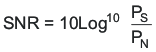
SNR is either given in units of dBc (dB to carrier) when the absolute power of the fundamental is used as the reference, or dBFS (dB to full-scale) when the power of the fundamental is extrapolated to the converter full-scale range.
Signal-to-Noise and Distortion (SINAD) – SINAD is the ratio of the power of the fundamental (PS) to the power of all the other spectral components including noise (PN) and distortion (PD), but excluding dc.
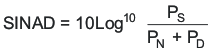
SINAD is either given in units of dBc (dB to carrier) when the absolute power of the fundamental is used as the reference, or dBFS (dB to full-scale) when the power of the fundamental is extrapolated to the converter full-scale range.
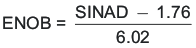
Effective Number of Bits (ENOB) – ENOB is a measure of the converter performance as compared to the theoretical limit based on quantization noise.
Total Harmonic Distortion (THD) – THD is the ratio of the power of the fundamental (PS) to the power of the first nine harmonics (PD).
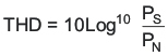
THD is typically given in units of dBc (dB to carrier).
Spurious-Free Dynamic Range (SFDR) – The ratio of the power of the fundamental to the highest other spectral component (either spur or harmonic). SFDR is typically given in units of dBc (dB to carrier).
Two-Tone Intermodulation Distortion – IMD3 is the ratio of the power of the fundamental (at frequencies f1 and f2) to the power of the worst spectral component at either frequency 2f1 – f2 or 2f2 – f1. IMD3 is either given in units of dBc (dB to carrier) when the absolute power of the fundamental is used as the reference, or dBFS (dB to full-scale) when the power of the fundamental is extrapolated to the converter full-scale range.
DC Power-Supply Rejection Ratio (DC PSRR) – DC PSSR is the ratio of the change in offset error to a change in analog supply voltage. The dc PSRR is typically given in units of mV/V.
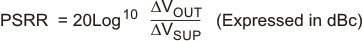
AC Power-Supply Rejection Ratio (AC PSRR) – AC PSRR is the measure of rejection of variations in the supply voltage by the ADC. If ΔVSUP is the change in supply voltage and ΔVOUT is the resultant change of the ADC output code (referred to the input), then:
Voltage Overload Recovery – The number of clock cycles taken to recover to less than 1% error after an overload on the analog inputs. This is tested by separately applying a sine wave signal with 6 dB positive and negative overload. The deviation of the first few samples after the overload (from the expected values) is noted.
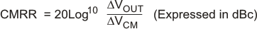
Common-Mode Rejection Ratio (CMRR) – CMRR is the measure of rejection of variation in the analog input common-mode by the ADC. If ΔVCM_IN is the change in the common-mode voltage of the input terminals and ΔVOUT is the resulting change of the ADC output code (referred to the input), then:
Crosstalk (only for multi-channel ADCs) – This is a measure of the internal coupling of a signal from an adjacent channel into the channel of interest. It is specified separately for coupling from the immediate neighboring channel (near-channel) and for coupling from channel across the package (far-channel). It is usually measured by applying a full-scale signal in the adjacent channel. Crosstalk is the ratio of the power of the coupling signal (as measured at the output of the channel of interest) to the power of the signal applied at the adjacent channel input. It is typically expressed in dBc.
11.2 Receiving Notification of Documentation Updates
To receive notification of documentation updates, navigate to the device product folder on ti.com. In the upper right corner, click on Alert me to register and receive a weekly digest of any product information that has changed. For change details, review the revision history included in any revised document.
11.3 Support Resources
TI E2E™ support forums are an engineer's go-to source for fast, verified answers and design help — straight from the experts. Search existing answers or ask your own question to get the quick design help you need.
Linked content is provided "AS IS" by the respective contributors. They do not constitute TI specifications and do not necessarily reflect TI's views; see TI's Terms of Use.
11.4 Trademarks
PowerPAD™ is a trademark of Texas Instruments Incorporated.
TI E2E™ are trademarks of Texas Instruments.
All trademarks are the property of their respective owners.
11.5 Electrostatic Discharge Caution
 |
This integrated circuit can be damaged by ESD. Texas Instruments recommends that all integrated circuits be handled with appropriate precautions. Failure to observe proper handling and installation procedures can cause damage. |
| ESD damage can range from subtle performance degradation to complete device failure. Precision integrated circuits may be more susceptible to damage because very small parametric changes could cause the device not to meet its published specifications. |
11.6 Glossary
-
TI Glossary
This glossary lists and explains terms, acronyms, and definitions.
12 Mechanical, Packaging, and Orderable Information
The following pages include mechanical, packaging, and orderable information. This information is the most current data available for the designated devices. This data is subject to change without notice and revision of this document. For browser-based versions of this data sheet, refer to the left-hand navigation.
IMPORTANT NOTICE AND DISCLAIMER
TI PROVIDES TECHNICAL AND RELIABILITY DATA (INCLUDING DATASHEETS), DESIGN RESOURCES (INCLUDING REFERENCE DESIGNS), APPLICATION OR OTHER DESIGN ADVICE, WEB TOOLS, SAFETY INFORMATION, AND OTHER RESOURCES “AS IS” AND WITH ALL FAULTS, AND DISCLAIMS ALL WARRANTIES, EXPRESS AND IMPLIED, INCLUDING WITHOUT LIMITATION ANY IMPLIED WARRANTIES OF MERCHANTABILITY, FITNESS FOR A PARTICULAR PURPOSE OR NON-INFRINGEMENT OF THIRD PARTY INTELLECTUAL PROPERTY RIGHTS.
These resources are intended for skilled developers designing with TI products. You are solely responsible for (1) selecting the appropriate TI products for your application, (2) designing, validating and testing your application, and (3) ensuring your application meets applicable standards, and any other safety, security, or other requirements. These resources are subject to change without notice. TI grants you permission to use these resources only for development of an application that uses the TI products described in the resource. Other reproduction and display of these resources is prohibited. No license is granted to any other TI intellectual property right or to any third party intellectual property right. TI disclaims responsibility for, and you will fully indemnify TI and its representatives against, any claims, damages, costs, losses, and liabilities arising out of your use of these resources.
TI’s products are provided subject to TI’s Terms of Sale (www.ti.com/legal/termsofsale.html) or other applicable terms available either on ti.com or provided in conjunction with such TI products. TI’s provision of these resources does not expand or otherwise alter TI’s applicable warranties or warranty disclaimers for TI products.
Mailing Address: Texas Instruments, Post Office Box 655303, Dallas, Texas 75265
Copyright © 2022, Texas Instruments Incorporated