SBAS653B April 2014 – October 2020 ADS4245-EP
PRODUCTION DATA
- 1 Features
- 2 Applications
- 3 Description
- 4 Revision History
- 5 Pin Configuration and Functions
-
6 Specifications
- 6.1 Absolute Maximum Ratings
- 6.2 ESD Ratings
- 6.3 Recommended Operating Conditions
- 6.4 Thermal Information
- 6.5 Electrical Characteristics:
- 6.6 Electrical Characteristics: General
- 6.7 Digital Characteristics
- 6.8 Timing Characteristics: LVDS And CMOS Modes
- 6.9 Typical Characteristics:
- 6.10 Typical Characteristics: General
- 6.11 Typical Characteristics: Contour
-
7 Detailed Description
- 7.1 Overview
- 7.2 Functional Block Diagram
- 7.3 Feature Description
- 7.4 Device Functional Modes
- 7.5 Serial Register Map
- 7.6 Description Of Serial Registers
- 8 Application Information Disclaimer
- 9 Power Supply Recommendations
- 10Layout
- 11Device and Documentation Support
- 12Mechanical, Packaging, and Orderable Information
Package Options
Mechanical Data (Package|Pins)
- RGC|64
Thermal pad, mechanical data (Package|Pins)
- RGC|64
Orderable Information
3 Description
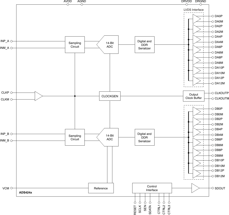
The ADS4245 is a low-speed variant of the ADS42xx ultralow-power family of dual-channel, 14-bit analog-to-digital converters (ADCs). Innovative design techniques are used to achieve high-dynamic performance, while consuming extremely low power with 1.8V supply. This topology makes the ADS4245 well-suited for multi-carrier, wide-bandwidth communications applications.
The ADS4245 has gain options that can be used to improve SFDR performance at lower full-scale input ranges. These device includes a dc offset correction loop that can be used to cancel the ADC offset. Both DDR (double data rate) LVDS and parallel CMOS digital output interfaces are available in a compact VQFN-64 PowerPAD™ package.
The device includes internal references while the traditional reference pins and associated decoupling capacitors have been eliminated. The ADS4245 is specified over the military temperature range (–55°C to 125°C).
| ORDER NUMBER | PACKAGE(1) | BODY SIZE |
|---|---|---|
| ADS4245MRGC25EP | VQFN (64) | 9mm × 9mm |
 Block Diagram