SBAS653B April   2014  – October 2020 ADS4245-EP

PRODUCTION DATA  

  1. Features
  2. Applications
  3. Description
  4. Revision History
  5. Pin Configuration and Functions
  6. Specifications
    1. 6.1  Absolute Maximum Ratings
    2. 6.2  ESD Ratings
    3. 6.3  Recommended Operating Conditions
    4. 6.4  Thermal Information
    5. 6.5  Electrical Characteristics:
    6. 6.6  Electrical Characteristics: General
    7. 6.7  Digital Characteristics
    8. 6.8  Timing Characteristics: LVDS And CMOS Modes
    9. 6.9  Typical Characteristics:
    10. 6.10 Typical Characteristics: General
    11. 6.11 Typical Characteristics: Contour
  7. Detailed Description
    1. 7.1 Overview
    2. 7.2 Functional Block Diagram
    3. 7.3 Feature Description
    4. 7.4 Device Functional Modes
      1. 7.4.1 Digital Functions
      2. 7.4.2 Gain For SFDR/SNR Trade-Off
      3. 7.4.3 Offset Correction
      4. 7.4.4 Power-Down
        1. 7.4.4.1 Global Power-Down
        2. 7.4.4.2 Channel Standby
        3. 7.4.4.3 Input Clock Stop
      5. 7.4.5 Digital Output Information
        1. 7.4.5.1 Output Interface
        2. 7.4.5.2 DDR LVDS Outputs
        3. 7.4.5.3 LVDS Buffer
        4. 7.4.5.4 Parallel CMOS Interface
        5. 7.4.5.5 CMOS Interface Power Dissipation
        6. 7.4.5.6 Multiplexed Mode Of Operation
        7. 7.4.5.7 Output Data Format
      6. 7.4.6 Device Configuration
        1. 7.4.6.1 Parallel Configuration Only
        2. 7.4.6.2 Serial Interface Configuration Only
        3. 7.4.6.3 Using Both Serial Interface And Parallel Controls
        4. 7.4.6.4 Parallel Configuration Details
        5. 7.4.6.5 Serial Interface Details
          1. 7.4.6.5.1 Register Initialization
          2. 7.4.6.5.2 Serial Register Readout
    5. 7.5 Serial Register Map
    6. 7.6 Description Of Serial Registers
  8. Application Information Disclaimer
    1. 8.1 Application Information
      1. 8.1.1 Clock Input
    2. 8.2 Typical Applications
      1. 8.2.1 Analog Input
        1. 8.2.1.1 Design Requirements for Drive Circuits
        2. 8.2.1.2 Detailed Design Procedure
        3. 8.2.1.3 Application Curves
  9. Power Supply Recommendations
  10. 10Layout
    1. 10.1 Layout Guidelines
      1. 10.1.1 Grounding
      2. 10.1.2 Supply Decoupling
      3. 10.1.3 Exposed Pad
      4. 10.1.4 Routing Analog Inputs
    2. 10.2 Layout Example
  11. 11Device and Documentation Support
    1. 11.1 Device Support
      1. 11.1.1 Device Support
        1. 11.1.1.1 Definition Of Specifications
    2. 11.2 Receiving Notification of Documentation Updates
    3. 11.3 Support Resources
    4. 11.4 Trademarks
    5. 11.5 Electrostatic Discharge Caution
    6. 11.6 Glossary
  12. 12Mechanical, Packaging, and Orderable Information

Package Options

Mechanical Data (Package|Pins)
Thermal pad, mechanical data (Package|Pins)
Orderable Information

Parallel CMOS Interface

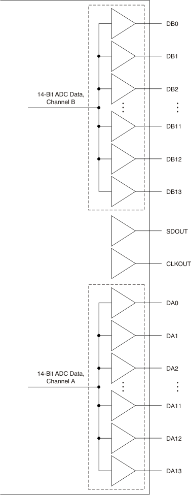
In the CMOS mode, each data bit is output on separate terminals as CMOS voltage level, every clock cycle, as Figure 7-6 shows. The rising edge of the output clock CLKOUT can be used to latch data in the receiver. It is recommended to minimize the load capacitance of the data and clock output terminals by using short traces to the receiver. Furthermore, match the output data and clock traces to minimize the skew between them.
GUID-3B9787FB-FF8A-4BC1-A949-09D4AFE5C55A-low.gif Figure 7-6 CMOS Outputs