SLAS904F October 2012 – May 2016 ADS42LB49 , ADS42LB69
PRODUCTION DATA.
- 1 Features
- 2 Applications
- 3 Description
- 4 Revision History
- 5 Pin Configuration and Functions
-
6 Specifications
- 6.1 Absolute Maximum Ratings
- 6.2 ESD Ratings
- 6.3 Recommended Operating Conditions
- 6.4 Thermal Information
- 6.5 Electrical Characteristics: ADS42LB69 (16-Bit)
- 6.6 Electrical Characteristics: ADS42LB49 (14-Bit)
- 6.7 Electrical Characteristics: General
- 6.8 Digital Characteristics
- 6.9 Timing Requirements: General
- 6.10 Timing Requirements: DDR LVDS Mode
- 6.11 Timing Requirements: QDR LVDS Mode
- 6.12 Typical Characteristics: ADS42LB69
- 6.13 Typical Characteristics: ADS42LB49
- 6.14 Typical Characteristics: Common
- 6.15 Typical Characteristics: Contour
- 7 Parameter Measurement Information
-
8 Detailed Description
- 8.1 Overview
- 8.2 Functional Block Diagrams
- 8.3 Feature Description
- 8.4 Device Functional Modes
- 8.5 Programming
- 8.6
Register Maps
- 8.6.1
Description of Serial Interface Registers
- 8.6.1.1 Register 6 (offset = 06h) [reset = 80h]
- 8.6.1.2 Register 7 (offset = 07h) [reset = 00h]
- 8.6.1.3 Register 8 (offset = 08h) [reset = 00h]
- 8.6.1.4 Register B (offset = 0Bh) [reset = 00h]
- 8.6.1.5 Register C (offset = 0Ch) [reset = 00h]
- 8.6.1.6 Register D (offset = 0Dh) [reset = 6Ch]
- 8.6.1.7 Register F (offset = 0Fh) [reset = 00h]
- 8.6.1.8 Register 10 (offset = 10h) [reset = 00h]
- 8.6.1.9 Register 11 (offset = 11h) [reset = 00h]
- 8.6.1.10 Register 12 (offset = 12h) [reset = 00h]
- 8.6.1.11 Register 13 (offset = 13h) [reset = 00h]
- 8.6.1.12 Register 14 (offset = 14h) [reset = 00h]
- 8.6.1.13 Register 15 (offset = 15h) [reset = 00h]
- 8.6.1.14 Register 16 (offset = 16h) [reset = 00h]
- 8.6.1.15 Register 17 (offset = 17h) [reset = 00h]
- 8.6.1.16 Register 18 (offset = 18h) [reset = 00h]
- 8.6.1.17 Register 1F (offset = 1Fh) [reset = 7Fh]
- 8.6.1.18 Register 20 (offset = 20h) [reset = 00h]
- 8.6.1
Description of Serial Interface Registers
- 9 Application and Implementation
- 10Power Supply Recommendations
- 11Layout
- 12Device and Documentation Support
- 13Mechanical, Packaging, and Orderable Information
Package Options
Mechanical Data (Package|Pins)
- RGC|64
Thermal pad, mechanical data (Package|Pins)
- RGC|64
Orderable Information
11 Layout
11.1 Layout Guidelines
- The length of the positive and negative traces of a differential pair must be matched to within 2 mils of each other.
- Each differential pair length must be matched within 10 mils of each other.
- When the ADC is used on the same printed circuit board (PCB) with a digital intensive component [such as a field-programmable gate array (FPGA) or application-specific integrated circuit (ASIC)], use separate digital and analog ground planes to minimize undesired coupling. Note that these ground planes must not overlap.
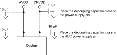
- Connect decoupling capacitors directly to ground and place these capacitors close to the ADC power pins and the power-supply pins to filter high-frequency current transients directly to the ground plane, as illustrated in Figure 126.
- Ground and power planes must be wide enough to keep the impedance very low. In a multilayer PCB, dedicate one layer to ground and another to power planes.
 Figure 126. Recommended Placement of Power-Supply Decoupling Capacitors
11.2 Layout Example
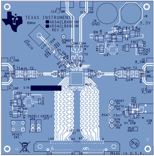
 Figure 127. Example Layout
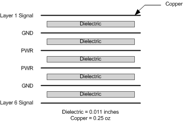
 Figure 128. Example PCB Layer Stack