SBAS603B April   2013  – November 2020 ADS4449

PRODUCTION DATA  

  1. Features
  2. Applications
  3. Description
  4. Revision History
  5. Pin Configuration and Functions
  6. Specifications
    1. 6.1  Absolute Maximum Ratings
    2. 6.2  ESD Ratings
    3. 6.3  Recommended Operating Conditions
    4. 6.4  Thermal Information
    5. 6.5  Electrical Characteristics
    6. 6.6  Digital Characteristics
    7. 6.7  Timing Requirements
    8. 6.8  Timing Characteristics, Serial interface
    9. 6.9  Typical Characteristics
    10. 6.10 Typical Characteristics: Contour
  7. Parameter Measurement Information
    1. 7.1 LVDS Output Timing
  8. Detailed Description
    1. 8.1 Overview
    2. 8.2 Functional Block Diagram
    3. 8.3 Feature Description
      1. 8.3.1 Overrange Indication (OVRxx)
      2. 8.3.2 Gain for SFDR and SNR Trade-Off
    4. 8.4 Device Functional Modes
      1. 8.4.1 Special Performance Modes
      2. 8.4.2 Digital Output Information
        1. 8.4.2.1 DDR LVDS Outputs
          1. 8.4.2.1.1 LVDS Output Data and Clock Buffers
          2. 8.4.2.1.2 Output Data Format
      3. 8.4.3 Using High SNR Mode Register Settings
      4. 8.4.4 Input Common Mode
    5. 8.5 Programming
      1. 8.5.1 Serial Interface
        1. 8.5.1.1 Register Initialization
        2. 8.5.1.2 Serial Register Readout
    6. 8.6 Register Maps
      1. 8.6.1 Register Description
        1. 8.6.1.1  Register Address 00h (Default = 00h)
        2. 8.6.1.2  Register Address 01h (Default = 00h)
        3. 8.6.1.3  Register Address 25h (Default = 00h)
        4. 8.6.1.4  Register Address 2bh (Default = 00h)
        5. 8.6.1.5  Register Address 31h (Default = 00h)
        6. 8.6.1.6  Register Address 37h (Default = 00h)
        7. 8.6.1.7  Register Address 3dh (Default = 00h)
        8. 8.6.1.8  Register Address 3fh (Default = 00h)
        9. 8.6.1.9  Register Address 40h (Default = 00h)
        10. 8.6.1.10 Register Address 42h (Default = 00h)
        11. 8.6.1.11 Register Address 45h (Default = 00h)
        12. 8.6.1.12 Register Address 4ah (Defalut = 00h)
        13. 8.6.1.13 Register Address 62h (Default = 00h)
        14. 8.6.1.14 Register Address 7ah (Default = 00h)
        15. 8.6.1.15 Register Address 92h (Default = 00h)
        16. 8.6.1.16 Register Address A9h (Default = 00h)
        17. 8.6.1.17 Register Address Ach (Default = 00h)
        18. 8.6.1.18 Register Address C3h (Default = 00h)
        19. 8.6.1.19 Register Address C4h (Default = 00h)
        20. 8.6.1.20 Register Address Cfh (Default = 00h)
        21. 8.6.1.21 Register Address D6h (Default = 00h)
        22. 8.6.1.22 Register Address D7h (Default = 00h)
        23. 8.6.1.23 Register Address F1h (Default = 00h)
        24. 8.6.1.24 Register Address 58h (Default = 00h)
        25. 8.6.1.25 Register Address 59h (Default = 00h)
        26. 8.6.1.26 Register Address 70h (Default = 00h)
        27. 8.6.1.27 Register Address 71h (Default = 00h)
        28. 8.6.1.28 Register Address 88h (Default = 00h)
        29. 8.6.1.29 Register Address 89h (Default = 00h)
        30. 8.6.1.30 Register Address A0h (Default = 00h)
        31. 8.6.1.31 Register Address A1h (Default = 00h)
        32. 8.6.1.32 Register Address Feh (Default = 00h)
  9. Application and Implementation
    1. 9.1 Application Information
    2. 9.2 Typical Application
      1. 9.2.1 Design Requirements
      2. 9.2.2 Detailed Design Procedure
      3. 9.2.3 Application Curves
      4. 9.2.4 Enabling 14-Bit Resolution
      5. 9.2.5 Analog Input
      6. 9.2.6 Drive Circuit Requirements
      7. 9.2.7 Clock Input
  10. 10Power Supply Recommendations
  11. 11Layout
    1. 11.1 Layout Guidelines
    2. 11.2 Layout Example
  12. 12Device and Documentation Support
    1. 12.1 Device Nomenclature
    2. 12.2 Documentation Support
      1. 12.2.1 Related Documentation
    3. 12.3 Receiving Notification of Documentation Updates
    4. 12.4 Support Resources
    5. 12.5 Trademarks
    6. 12.6 Electrostatic Discharge Caution
    7. 12.7 Glossary

Package Options

Mechanical Data (Package|Pins)
Thermal pad, mechanical data (Package|Pins)
Orderable Information

Typical Characteristics

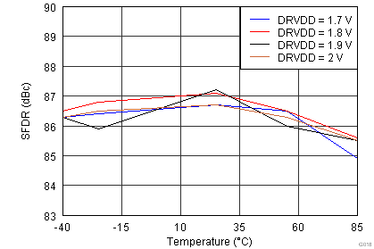
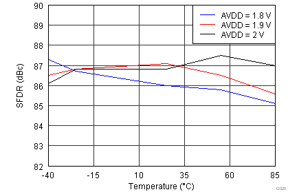
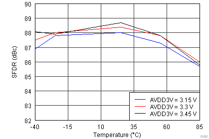
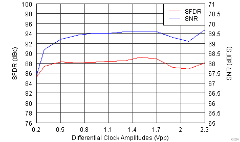
At 25°C, AVDD = 1.9 V, AVDD3V = 3.3 V, DRVDD = 1.8 V, rated sampling frequency, 0-dB gain, sine-wave input clock, 1.5-VPP differential clock amplitude, 50% clock duty cycle, –1-dBFS differential analog input, DDR LVDS output interface, and 32k-point FFT, unless otherwise noted.
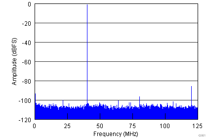
GUID-9E3BE7CD-0904-496A-9165-5ACD6873249F-low.png
fIN = 40 MHzSFDR = 84 dBcSNR = 71.1 dBFS
SINAD = 70.9 dBFSTHD = 84 dBc
Figure 6-2 FFT for 40-MHz Input Signal
GUID-4D101D89-E569-49B8-AADC-B856109E14B4-low.png
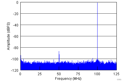
fIN = 100 MHzSFDR = 85 dBcSNR = 70.2 dBFS
SINAD = 70.1 dBFSTHD = 84 dBc
Figure 6-4 FFT for 100-MHz Input Signal
GUID-EEC27D93-02D3-4B81-A0B0-D6BCE277093D-low.png
fIN = 170 MHzSFDR = 89 dBcSNR = 69 dBFS
SINAD = 68.9 dBFSTHD = 85 dBc
Figure 6-6 FFT for 170-MHz Input Signal
GUID-92FDEAC3-3190-4F6B-B40E-73D5FF88B3D9-low.png
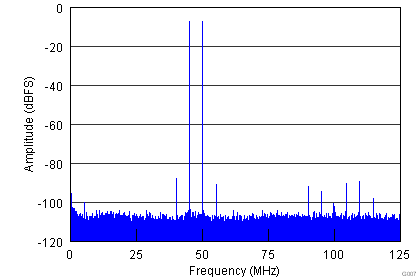
Each Tone at –7-dBFS Amplitude
fIN1 = 45 MHzfIN2 = 50 MHzSFDR = 92 dBFS
2-Tone IMD = 87 dBFS
Figure 6-8 FFT for Two-Tone Input Signal
GUID-9E2041F5-4282-48BB-8EB5-0D3F55C34976-low.png
Each Tone at –7-dBFS Amplitude
fIN1 = 185.1 MHzfIN2 = 190.1 MHzSFDR = 102 dBFS
2-Tone IMD = 97 dBFS
Figure 6-10 FFT for Two-Tone Input Signal
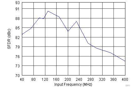
GUID-E3C0FFC4-2DBC-4366-84BC-3684125BA5D3-low.pngFigure 6-12 Spurious-Free Dynamic Range vs Input Frequency
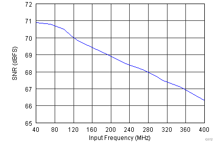
GUID-E78214AD-430D-46E4-8D0E-17CFB890E5B0-low.pngFigure 6-14 Signal-to-Noise Ratio vs Input Frequency
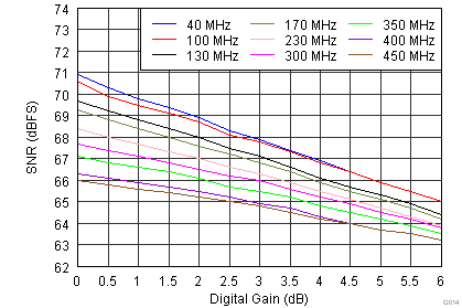
GUID-D1746510-6435-468F-81F6-26CD46F0D4D7-low.pngFigure 6-16 Signal-to-Noise Ratio vs Digital Gain
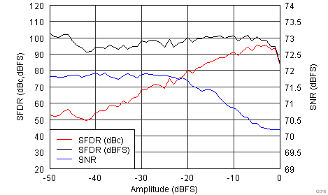
GUID-29D0080E-1248-4E56-894B-6E78833878FF-low.png
Input Frequency = 185 MHz
Figure 6-18 Performance vs Input Amplitude
GUID-0CCD635D-A523-4D88-95E4-D3BD7019BA22-low.png
Input Frequency = 185 MHz
Figure 6-20 Spurious-Free Dynamic Range vs DRVDD Supply and Temperature
GUID-97AF15BE-5270-4E98-8BF4-6F1AB4798944-low.png
Input Frequency = 185 MHz
Figure 6-22 Spurious-Free Dynamic Range vs AVDD Supply and Temperature
GUID-6CFD5D00-D844-4D60-BE5F-CFBC0EB38221-low.png
Input Frequency = 185 MHz
Figure 6-24 Spurious-Free Dynamic Range vs AVDD3V Supply and Temperature
GUID-E4A97017-BA09-46A5-9005-FA5A16389A2A-low.png
Input Frequency = 185 MHz
Figure 6-26 Performance vs Clock Amplitude
GUID-FA101B82-C080-4021-8A2E-50FAA9FC9DAB-low.png
Input Frequency = 185 MHz
50-mVPP Signal Superimposed on VCM
Figure 6-28 Common-Mode Rejection Ratio Spectrum
GUID-DE7DD722-D970-4D7B-AF4F-493E19CB7CDE-low.png
Input Frequency = 10 MHz
50-mVPP Signal Superimposed on Supply
Figure 6-30 Power-Supply Rejection Ratio Spectrum for AVDD
GUID-9EF7C102-F4D6-4A3F-A04E-7F98BD98EF4C-low.png
Input Frequency = 185 MHz
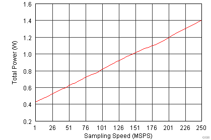
Figure 6-32 Total Power vs Sampling Frequency
GUID-8311DFB2-D276-43A8-9D90-35A262FC52F0-low.png
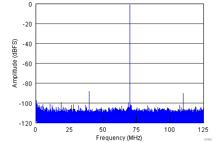
fIN = 70 MHzSFDR = 87 dBcSNR = 70.9 dBFS
SINAD = 70.8 dBFSTHD = 84 dBc
Figure 6-3 FFT for 70-MHz Input Signal
GUID-ADEB1D4E-F8C8-450B-81AE-9CB64A963844-low.png
fIN = 140 MHzSFDR = 87 dBcSNR = 69.7 dBFS
SINAD = 69.6 dBFSTHD = 84 dBc
Figure 6-5 FFT for 140-MHz Input Signal
GUID-A6CDE070-6555-4605-94C7-F79EFF7183D8-low.png
fIN = 230 MHzSFDR = 86 dBcSNR = 68.9 dBFS
SINAD = 68.5 dBFSTHD = 84 dBc
Figure 6-7 FFT for 230-MHz Input Signal
GUID-0B8C5100-FB5A-4406-9C9A-9F8CFD36ED70-low.png
Each Tone at –36-dBFS Amplitude
fIN1 = 45 MHzfIN2 = 50 MHzSFDR = 99 dBFS
2-Tone IMD = 99 dBFS
Figure 6-9 FFT for Two-Tone Input Signal
GUID-87CFF3A9-E466-429E-9D1C-2DD17DD39EE3-low.png
Each Tone at –36-dBFS Amplitude
fIN1 = 185.1 MHzfIN2 = 190.1 MHzSFDR = 100 dBFS
2-Tone IMD = 101 dBFS
Figure 6-11 FFT for Two-Tone Input Signal
GUID-41A84820-FF38-4DB8-A35D-92569E13A0C9-low.png
Input Frequency = 170 MHz
Figure 6-13 HD2 Distribution over Multiple Devices
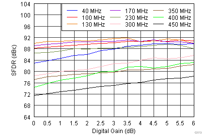
GUID-6588420F-7A40-4078-A700-CD9D1447ED33-low.pngFigure 6-15 Spurious-Free Dynamic Range vs Digital Gain
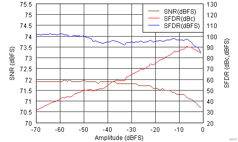
GUID-31B29A42-5C78-4BD5-BD51-FE05AFDAFA7D-low.png
Input Frequency = 70 MHz
Figure 6-17 Performance vs Input Amplitude
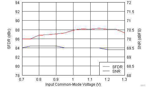
GUID-6FF082E1-4A78-4786-A6E6-B6CC9DC4B018-low.png
Input Frequency = 185 MHz
Figure 6-19 Performance vs Input Common-Mode Voltage
GUID-E985F682-ED70-430C-8093-214A25493603-low.png
Input Frequency = 185 MHz
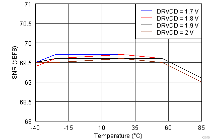
Figure 6-21 Signal-to-Noise Ratio vs DRVDD Supply and Temperature
GUID-D24B9053-7208-46C4-8D4E-64257AAE4C72-low.png
Input Frequency = 185 MHz
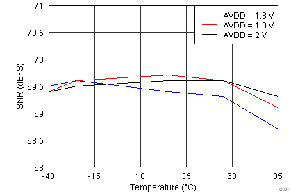
Figure 6-23 Signal-to-Noise Ratio vs AVDD Supply and Temperature
GUID-64F5E5DA-8392-482A-A310-9BFE454FAE80-low.png
Input Frequency = 185 MHz
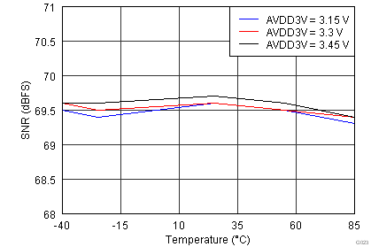
Figure 6-25 Signal-to-Noise Ratio vs AVDD3V Supply and Temperature
GUID-56CB8441-C86E-443F-ADAF-6CA361FB5A14-low.png
Input Frequency = 185 MHz
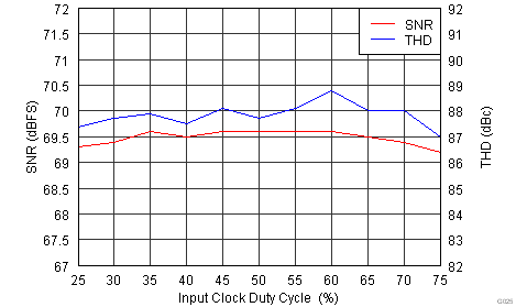
Figure 6-27 Performance vs Clock Duty Cycle
GUID-378781BC-1004-4CA8-BF89-C42E95CC0191-low.png
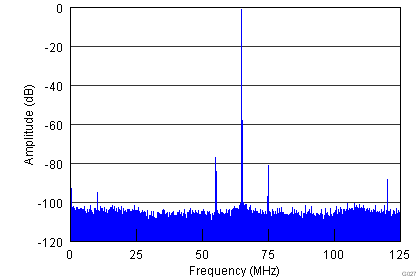
fIN = 185 MHzAmplitude (fIN – fCM) = –80.9 dBFS
Amplitude (fIN) = –1 dBFSAmplitude (fCM) = –95 dBFS
fCM = 10 MHz, 50 mVPPAmplitude (fIN + fCM) = –77.2 dBFS
SFDR = 76 dBc
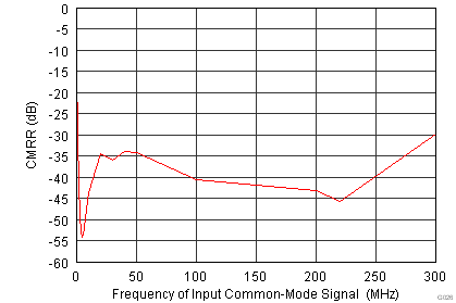
Figure 6-29 Common-Mode Rejection Ratio vs Test Signal Frequency
GUID-E15810FB-C3F1-4A20-8801-409A106A8FDA-low.png
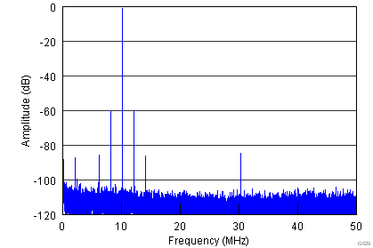
Amplitude (fIN) = –1 dBFSAmplitude (fPSRR) = –87 dBFS
fIN = 10 MHzAmplitude (fIN + fPSRR) = –60.6 dBFS
fPSRR = 2 MHz, 50 mVPPAmplitude (fIN – fPSRR) = –60 dBFS
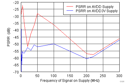
Figure 6-31 Power-Supply Rejection Ratio vs Test Signal Frequency
GUID-EB416069-FE79-4002-A381-5075FD094856-low.png
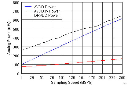
Input Frequency = 185 MHz
Figure 6-33 Power Breakup vs Sampling Frequency