SBASAF8 September 2021 ADS52J91
PRODUCTION DATA
- 1Features
- 2Applications
- 3Description
- 4Revision History
- 5Description (continued)
- 6Device and Documentation Support
- 7Mechanical, Packaging, and Orderable Information
Package Options
Mechanical Data (Package|Pins)
- ZZE|198
Thermal pad, mechanical data (Package|Pins)
Orderable Information
3 Description
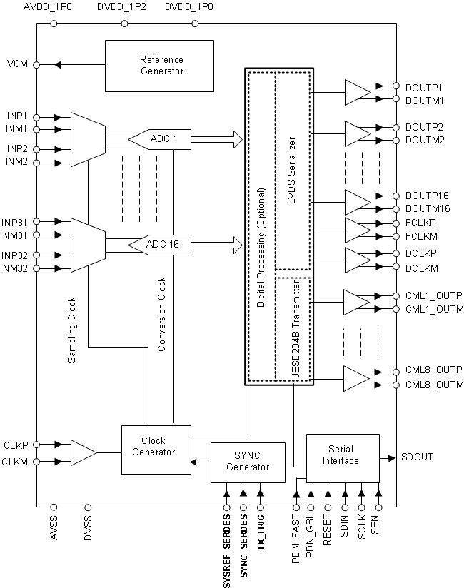
The ADS52J91 is a low-power, high-performance, 16-channel, analog-to-digital converter (ADC). The conversion rate of each ADC goes up to a maximum of 125 MSPS in 10-bit mode. The maximum conversion rate reduces when the ADC resolution is set to a higher value.
The device can be configured to accept 8, 16, or 32 inputs. In 32-input mode, each ADC alternately samples and converts two different inputs each at an effective sampling rate that is half of the ADC conversion rate. In 8-bit input mode, two ADCs convert the same input in an interleaved manner, resulting in an effective sampling rate that is twice the ADC conversion rate. The ADC is designed to scale its power with the conversion rate.
| PART NUMBER | PACKAGE | BODY SIZE (NOM) |
|---|---|---|
| ADS52J91 | NFBGA (198) | 9.00 mm × 15.00 mm |
 Simplified Schematic