SLAS611C October 2009 – January 2016 ADS5400
PRODUCTION DATA.
- 1 Features
- 2 Applications
- 3 Description
- 4 Revision History
- 5 Pin Configuration and Functions
- 6 Specifications
-
7 Detailed Description
- 7.1 Overview
- 7.2 Functional Block Diagram
- 7.3 Feature Description
- 7.4 Device Functional Modes
- 7.5 Programming
- 7.6 Register Maps
- 8 Application and Implementation
- 9 Power Supply Recommendations
- 10Layout
- 11Device and Documentation Support
- 12Mechanical, Packaging, and Orderable Information
Package Options
Mechanical Data (Package|Pins)
- PZP|100
Thermal pad, mechanical data (Package|Pins)
- PZP|100
Orderable Information
8 Application and Implementation
NOTE
Information in the following applications sections is not part of the TI component specification, and TI does not warrant its accuracy or completeness. TI’s customers are responsible for determining suitability of components for their purposes. Customers should validate and test their design implementation to confirm system functionality.
8.1 Application Information
In the design of any application involving a high-speed data converter, particular attention should be paid to the design of the analog input, the clocking solution, and careful layout of the clock and analog signals. The ADS5400 evaluation module (EVM) is one practical example of the design of the analog input circuit and clocking solution, as well as a practical example of good circuit board layout practices around the ADC.
8.2 Typical Application
The analog inputs of the ADS5400 must be fully differential and biased to an appropriate common mode voltage, VCM. It is rare that the end equipment will have a signal that already meets the requisite amplitude and common mode and is fully differential. Therefore, there will be a signal conditioning circuit for the analog input. If the amplitude of the input circuit is such that no gain is needed to make full use of the full-scale range of the ADC, then a transformer coupled circuit as used on the EVM may be used with good results. The transformer coupling is inherently low-noise, and inherently AC-coupled so that the signal may be biased to VCM after the transformer coupling.
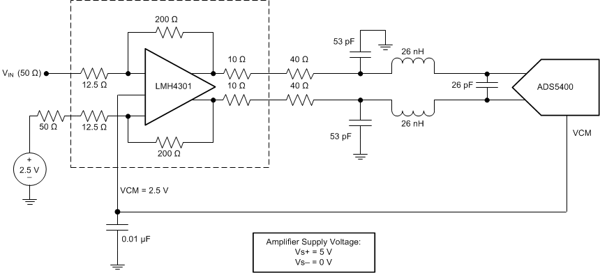
If signal gain is required, or the input bandwidth is to include the spectrum all the way down to DC such that AC coupling is not possible, then an amplifier-based signal conditioning circuit would be required. Figure 37 shows LMH3401 interfaced with ADS5400. LMH3401 is configured to have to Single-Ended input with a differential outputs follow by 1st Nyquist based low pass filter with 400 MHz bandwidth. Figure 37 also shows the power supply recommendations for the amplifier.
 Figure 37. ADS5400 Input Circuit Using an LMH3401 Fully Differential Amplifier
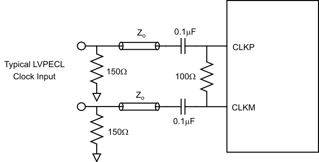
Clocking a High Speed ADC such as the ADS5400 requires a fully differential clock signal from a clean, low-jitter clock source and driven by an appropriate clock buffer, often with LVPECL or LVDS signaling levels. The sample clock must be biased up to the appropriate common-mode voltage, and the ADS5400 will internally bias the clock to the appropriate common-mode voltage if the clock signal is AC-coupled as shown in Figure 38.
 Figure 38. Recommended Differential Clock Driving Circuit
8.2.1 Design Requirements
The ADS5400 requires a fully differential analog input with a full-scale range not to exceed 2 V peak to peak differential, biased to a common mode voltage of 2.5 V. In addition the input circuit must provide proper transmission line termination (or proper load resistors in an amplifier-based solution) so the input of the impedance of the ADC analog inputs should be considered as well.
The ADS5400 is capable of a typical SNR of 58.5 dBFS for input frequencies of about 125 MHz, which is well under the Nyquist limit for this ADC operating at 1000 Msps. The amplifier and clocking solution will have a direct impact on performance in terms of SNR, so the amplifier and clocking solution should be selected such that the SNR performance of at least 58 dBFS is preserved.
8.2.2 Detailed Design Procedure
8.2.2.1 Clocking Source for ADS5400
The signal to noise ratio of the ADC is limited by three different factors: the quantization noise, the thermal noise, and the total jitter of the sample clock. Quantization noise is driven by the resolution of the ADC, which is 12 bits for the ADS5400. Thermal noise is typically not noticeable in high speed pipelined converters such as the ADS5400, but may be estimated by looking at the signal to noise ratio of the ADC with very low input frequencies and using Equation 2 to solve for thermal noise. (For this estimation, we will take thermal noise to be zero. The lowest frequency for which SNR is specified is 125 MHz. If we had an SNR specification for input frequencies around 5 MHz then that SNR would be a good approximation for SNR due to thermal noise. This would be just an approximation, and the lower the input frequency that has an SNR specification the better this approximation would be.) The thermal noise limits the SNR at low input frequencies while the clock jitter sets the SNR for higher input frequencies. For ADCs with higher resolution and typical SNR of 75 dBFS or so, thermal noise would be more of a factor in overall performance. Quantization noise is also a limiting factor for SNR, as the theoretical maximum achievable SNR as a function of the number of bits of resolution is set by Equation 1.

where
- N = number of bits resolution.
For a 12-bit ADC, the maximum SNR = 1.76 + (6.02 × 12) = 74 dB. This is the number that we shall enter into Equation 2 for quantization noise as we solve for total SNR for different amounts of clock jitter using Equation 2.

The SNR limitation due to sample clock jitter can be calculated by Equation 3.

It is important to note that the clock jitter in Equation 3 is the total amount of clock jitter, whether the jitter source is internal to the ADC itself or external due to the clocking source. The total clock jitter (TJitter) has two components – the internal aperture jitter (125 fs for ADS5400) which is set by the noise of the clock input buffer, and the external clock jitter from the clocking source and all associated buffering of the clock signal. Total clock jitter can be calculated from the aperture jitter and the external clock jitter as in Equation 4.

External clock jitter can be minimized by using high quality clock sources and jitter cleaners as well as bandpass filters at the clock input while a faster clock slew rate may at times also improve the ADC aperture jitter slightly.
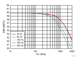
The ADS5400 has an internal aperture jitter of 125 fs, which is largely fixed. The SNR depending on amount of external jitter for different input frequencies is shown in Figure 39. Often the design requirements will list a target SNR for a system, and Equation 2 through Equation 4 are then used to calculate the external clock jitter needed from the clocking solution to meet the system objectives.
Figure 39 shows that with an external clock jitter of 200 fs rms, the expected SNR of the ADS5400 would be greater than 58 dBFS at an input tone of 400 MHz, which is the assumed bandwidth for this design example. Having less external clock jitter such as 150 fs rms or even 100 fs rms would result in an SNR that would exceed our design target, but at possibly the expense of a more costly clocking solution. Having external clock jitter of much greater than 200 fs rms or more would fail to meet our design target.
8.2.2.2 Amplifier Selection
The amplifier and any input filtering will have its own SNR performance, and the SNR performance of the amplifier front end will combine with the SNR of the ADC itself to yield a system SNR that is less than that of the ADC itself. System SNR can be calculated from the SNR of the amplifier conditioning circuit and the overall ADC SNR as in Equation 5. In Equation 5, the SNR of the ADC would be the value derived from the datasheet specifications and the clocking derivation presented in the previous section.

The signal-to-noise ratio (SNR) of the amplifier and filter can be calculated from the noise specifications in the datasheet for the amplifier, the amplitude of the signal and the bandwidth of the filter. The noise from the amplifier is band-limited by the filter and the rolloff of the filter will depend on the order of the filter, so it is convenient to replace the filter rolloff with an equivalent brick-wall filter bandwidth. For example, a 1st order filter may be approximated by a brick-wall filter with bandwidth of 1.57 times the bandwidth of the 1st order filter. We will assume a 1st order filter for this design. The amplifier and filter noise can be calculated using Equation 6.

where
- VO= the amplifier output signal (which will be full scale input of the ADC expressed in rms)
- EFILTEROUT = ENAMPOUT × √ENB
- ENAMPOUT = the output noise density of the LMH3401 (3.4 nV/√Hz)
- ENB = the brick-wall equivalent noise bandwidth of the filter
In Equation 6, the parameters of the equation may be seen to be in terms of signal amplitude in the numerator and amplifier noise in the denominator, or SNR. For the numerator, use the full scale voltage specification of the ADS5400, or 2 V peal to peak differential. Because Equation 6 requires the signal voltage to be in rms, convert 2 VPP to 0.706 V rms.
The noise specification for the LMH3401 is listed as 3.4 nV/√Hz, therefore, use this value to integrate the noise component from DC out to the filter cutoff, using the equivalent brick wall filter of 400 MHz × 1.57, or 628 MHz. 3.4 nV/√Hz integrated over 628 MHz yields 85204 nV, or 85.204 µV.
Using 0.706 V rms for VO and 85.204 µV for EFILTEROUT, (see Equation 6) the SNR of the amplifier and filter as given by Equation 6 is approximately 78.4 dB.
Taking the SNR of the ADC as 58.8 dB from Figure 39, and SNR of the amplifier and filter as 78.4 dB, Equation 5 predicts the system SNR to be 58.75 dB. In other words, the SNR of the ADC and the SNR of the front end combine as the square root of the sum of squares, and because the SNR of the amplifier front end is much greater than the SNR of the ADC in this example, the SNR of the ADC dominates Equation 5 and the system SNR is almost the same as the SNR of the ADC. The assumed design requirement is 58 dB, and after a clocking solution was selected and an amplifier or filter solution was selected, the predicted SNR is 58.75 dBFS.
8.2.3 Application Curve
Figure 39 shows the SNR of the ADC as a function of clock jitter and input frequency for the ADS5400. This plot of curves take into account the aperture jitter of the ADC, the number of bits of resolution, and the thermal noise estimation so that Figure 39 may be used to predict SNR for a given input frequency and external clock jitter. Figure 39 then may be used to set the jitter requirement for the clocking solution for a given input bandwidth and given design goal for SNR.
 Figure 39. SNR vs Input Frequency and External Clock Jitter