SLAS611C October 2009 – January 2016 ADS5400
PRODUCTION DATA.
- 1 Features
- 2 Applications
- 3 Description
- 4 Revision History
- 5 Pin Configuration and Functions
- 6 Specifications
-
7 Detailed Description
- 7.1 Overview
- 7.2 Functional Block Diagram
- 7.3 Feature Description
- 7.4 Device Functional Modes
- 7.5 Programming
- 7.6 Register Maps
- 8 Application and Implementation
- 9 Power Supply Recommendations
- 10Layout
- 11Device and Documentation Support
- 12Mechanical, Packaging, and Orderable Information
Package Options
Mechanical Data (Package|Pins)
- PZP|100
Thermal pad, mechanical data (Package|Pins)
- PZP|100
Orderable Information
10 Layout
10.1 Layout Guidelines
The evaluation board provides a guideline of how to lay out the board to obtain the maximum performance from the ADS5400. General design rules, such as the use of multilayer boards, single ground plane for ADC ground connections, and local decoupling ceramic chip capacitors, should be applied. The input traces should be isolated from any external source of interference or noise, including the digital outputs as well as the clock traces. The clock signal traces should also be isolated from other signals, especially in applications where low jitter is required like high IF sampling. Besides performance-oriented rules, care must be taken when considering the heat dissipation of the device. The thermal heat sink should be soldered to the board as described in the PowerPAD™ Package section.
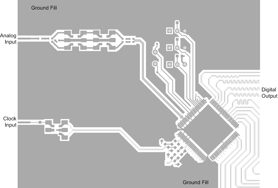
Figure 41 is a section of the layout of the ADS5400 that illustrates good layout practices for the clocking, analog input, and digital outputs. In this example, the analog input enters from the top left while the clocking enters from the left center, keeping the clock signal away from the analog signals so as to not allow coupling between the analog signal and the clock signal. One thing to notice on the layout of the differential traces is the symmetry of the trace routing between the two sides of the differential signals.
The digital outputs are routed off to the right, so as to keep the digital signals away from the analog inputs and away from the clock. Notice the circuitous routing added to some of the LVDS differential traces but not to others; this is the equalize the lengths of the routing across all of the LVDS traces so as to preserve the setup/hold timing at the end of the digital signal routings. If the timing closure in the receiving device (such as an FPGA or ASIC) has enough timing margin, then the circuitous routing to equalize trace lengths may not be necessary.
10.2 Layout Example
 Figure 41. Typical Layout of AS5400
10.3 PowerPAD™ Package
The PowerPAD package is a thermally enhanced standard-size IC package designed to eliminate the use of bulky heatsinks and slugs traditionally used in thermal packages. This package can be mounted using standard printed circuit board (PCB) assembly techniques, and can be removed or replaced using standard repair procedures.
The PowerPAD package is designed so that the leadframe die pad (or thermal pad) is exposed on the bottom of the IC. This provides an extremely low thermal resistance path between the die and the exterior of the package. The thermal pad on the bottom of the IC can then be soldered directly to the printed circuit board (PCB), using the PCB as a heatsink.
10.3.1 Assembly Process
- Prepare the PCB top-side etch pattern including etch for the leads as well as the thermal pad as illustrated in the Mechanical Data section.
- It is recommended to place a 9 × 9 array of 13-mil-diameter (0.33 mm) via holes under the package, with the middle 5 × 5 array of thermal vias exposed.
- Connect all holes (both those inside and outside the thermal pad area) to an internal copper plane (such as a ground plane).
- Do not use the typical web or spoke via-connection pattern when connecting the thermal vias to the ground plane. The spoke pattern increases the thermal resistance to the ground plane.
- The top-side solder mask should leave exposed the terminals of the package and the 5 × 5 via array thermal pad area (6 mm × 6 mm).
- Cover the entire bottom side of the PowerPAD vias to prevent solder wicking.
- Apply solder paste to the exposed thermal pad area and all of the package terminals.
For more detailed information regarding the PowerPAD package and its thermal properties, see either the PowerPAD Made Easy application brief (SLMA004) or the PowerPAD Thermally Enhanced Package application report (SLMA002).