SLAS611C October   2009  – January 2016 ADS5400

PRODUCTION DATA.  

  1. Features
  2. Applications
  3. Description
  4. Revision History
  5. Pin Configuration and Functions
  6. Specifications
    1. 6.1 Absolute Maximum Ratings
    2. 6.2 ESD Ratings
    3. 6.3 Recommended Operating Conditions
    4. 6.4 Thermal Information
    5. 6.5 Electrical Characteristics
    6. 6.6 Interleaving Adjustments
    7. 6.7 Timing Requirements
    8. 6.8 Switching Characteristics
    9. 6.9 Typical Characteristics
  7. Detailed Description
    1. 7.1 Overview
    2. 7.2 Functional Block Diagram
    3. 7.3 Feature Description
      1. 7.3.1  Input Configuration
      2. 7.3.2  Voltage Reference
      3. 7.3.3  Analog Input Over-Range Recovery Error
      4. 7.3.4  Clock Inputs
      5. 7.3.5  Over Range
      6. 7.3.6  Data Scramble
      7. 7.3.7  Test Patterns
      8. 7.3.8  Die Identification and Revision
      9. 7.3.9  Die Temperature Sensor
      10. 7.3.10 Interleaving
        1. 7.3.10.1 Gain Adjustment
        2. 7.3.10.2 Offset Adjustment
        3. 7.3.10.3 Input Clock Coarse Phase Adjustment
        4. 7.3.10.4 Input Clock Fine Phase Adjustment
    4. 7.4 Device Functional Modes
      1. 7.4.1 Output Bus and Clock Options
      2. 7.4.2 Reset and Synchronization
      3. 7.4.3 LVDS
    5. 7.5 Programming
      1. 7.5.1 Serial Interface
    6. 7.6 Register Maps
      1. 7.6.1 Serial Register Map
      2. 7.6.2 Description of Serial Registers
  8. Application and Implementation
    1. 8.1 Application Information
    2. 8.2 Typical Application
      1. 8.2.1 Design Requirements
      2. 8.2.2 Detailed Design Procedure
        1. 8.2.2.1 Clocking Source for ADS5400
        2. 8.2.2.2 Amplifier Selection
      3. 8.2.3 Application Curve
  9. Power Supply Recommendations
  10. 10Layout
    1. 10.1 Layout Guidelines
    2. 10.2 Layout Example
    3. 10.3 PowerPAD™ Package
      1. 10.3.1 Assembly Process
  11. 11Device and Documentation Support
    1. 11.1 Device Support
      1. 11.1.1 Device Nomenclature
    2. 11.2 Documentation Support
      1. 11.2.1 Related Documentation
    3. 11.3 Community Resources
    4. 11.4 Trademarks
    5. 11.5 Electrostatic Discharge Caution
    6. 11.6 Glossary
  12. 12Mechanical, Packaging, and Orderable Information

Package Options

Mechanical Data (Package|Pins)
Thermal pad, mechanical data (Package|Pins)
Orderable Information

9 Power Supply Recommendations

The ADS5400 uses three power supplies. For the analog portion of the design, a 5-V and 3.3-V supply (AVDD5 and AVDD3) are used, while the digital portion uses a 3.3-V supply (DVDD3). The use of low-noise power supplies with adequate decoupling is recommended. Linear supplies are preferred to switched supplies; switched supplies generate more noise components that can be coupled to the ADS5400. The PSRR value and the plot shown in Figure 40 were obtained without bulk supply decoupling capacitors. When bulk (0.1 μF) decoupling capacitors are used, the board-level PSRR is much higher than the stated value for the ADC. The power consumption of the ADS5400 does not change substantially over clock rate or input frequency as a result of the architecture and process.
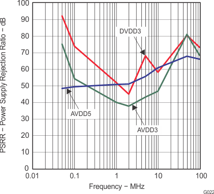
ADS5400 G022_LAS611.gif Figure 40. PSRR versus Supply Injected Frequency