SGLS378G March 2008 – October 2017 ADS5463-SP
PRODUCTION DATA.
- 1 Features
- 2 Applications
- 3 Description
- 4 Revision History
- 5 Pin Configuration and Functions
-
6 Specifications
- 6.1 Absolute Maximum Ratings
- 6.2 ESD Ratings
- 6.3 Recommended Operating Conditions
- 6.4 Thermal Information
- 6.5 Electrical Characteristics: ADS5463-RHA
- 6.6 Electrical Characteristics: ADS5463-RHA
- 6.7 Electrical Characteristics: ADS5463-RHA
- 6.8 Electrical Characteristics: ADS5463-SP
- 6.9 Electrical Characteristics: ADS5463-SP
- 6.10 Electrical Characteristics: ADS5463-SP
- 6.11 Timing Requirements
- 6.12 Typical Characteristics
- 7 Detailed Description
- 8 Application and Implementation
- 9 Power Supply Recommendations
- 10Layout
- 11Device and Documentation Support
- 12Mechanical, Packaging, and Orderable Information
Package Options
Mechanical Data (Package|Pins)
- HFG|84
Thermal pad, mechanical data (Package|Pins)
Orderable Information
8 Application and Implementation
NOTE
Information in the following applications sections is not part of the TI component specification, and TI does not warrant its accuracy or completeness. TI’s customers are responsible for determining suitability of components for their purposes. Customers should validate and test their design implementation to confirm system functionality.
8.1 Application Information
The ADS5463 is a 12-bit, 500-MSPS, monolithic-pipeline, analog-to-digital converter. Its bipolar analog core operates from 5-V and 3.3-V supplies, while the output uses a 3.3-V supply to provide LVDS-compatible outputs. The conversion process is initiated by the rising edge of the external input clock. The differential input signal is captured by the input track-and-hold (T&H), and the input sample is sequentially converted by a series of lower resolution stages, with the outputs combined in a digital correction logic block. Both the rising and the falling clock edges are used to propagate the sample through the pipeline every half clock cycle. This process results in a data latency of 3.5 clock cycles, after which the output data is available as a 12-bit parallel word, coded in offset binary format.
8.1.1 Input Configuration
The analog input for the ADS5463 consists of an analog pseudodifferential buffer followed by a bipolar transistor track-and-hold. The analog buffer isolates the source driving the input of the ADC from any internal switching. The input common mode is set internally through a 500-Ω resistor connected from 2.4 V to each of the inputs. This results in a differential input impedance of 1 kΩ.
For a full-scale differential input, each of the differential lines of the input signal (pins 17 and 18) swings symmetrically between 2.4 V + 0.55 V and 2.4 V – 0.55 V. This means that each input has a maximum signal swing of 1.1 Vpp for a total differential input signal swing of 2.2 Vpp. The maximum swing is determined by the internal reference voltage generator, eliminating the need for any external circuitry for this purpose.
The ADS5463 obtains optimum performance when the analog inputs are driven differentially. The circuit in Figure 15 shows one possible configuration using an RF transformer with termination either on the primary or on the secondary of the transformer. In addition, the evaluation module is configured with two back-to-back transformers, which also demonstrate good performance. If voltage gain is required, a step-up transformer can be used.
Besides the transformer configurations, Texas Instruments offers a wide selection of single-ended operational amplifiers that can be selected depending on the application. An RF gain-block amplifier, such as Texas Instruments' THS9001, also can be used for high-input-frequency applications. For large voltage gains at intermediate-frequencies in the 50-MHz – 500-MHz range, the configuration shown in Figure 16 can be used. The component values can be tuned for different intermediate frequencies. The example shown is located on the evaluation module and is tuned for an IF of 170 MHz. More information regarding this configuration can be found in the ADS5463 EVM User Guide (SLAU194) and the THS9001 50 MHz to 350 MHz Cascadeable Amplifier data sheet (SLOS426).
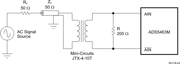 Figure 15. Converting a Single-Ended Input to a Differential Signal Using an RF Transformer
 Figure 16. Using the THS9001 IF Amplifier With the ADS5463
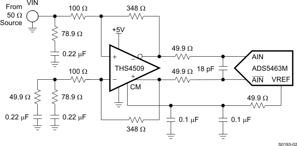 Figure 17. Using the THS4509 With the ADS5463
For applications requiring dc-coupling with the signal source, a differential input/differential output amplifier like the THS4509 (see Figure 17) is a good solution, as it minimizes board space and reduces the number of components.
In this configuration, the THS4509 amplifier circuit provides 10-dB of gain, converts the single-ended input to differential, and sets the proper input common-mode voltage to the ADS5463. The 50-Ω resistors and 18-pF capacitor between the THS4509 outputs and ADS5463 inputs (along with the input capacitance of the ADC) limit the bandwidth of the signal to about 70 MHz (–3 dB). Input termination is accomplished via the 78.9-Ω resistor and 0.22-μF capacitor to ground, in conjunction with the input impedance of the amplifier circuit. A 0.22-μF capacitor and 49.9-Ω resistor are inserted to ground across the 78.9-Ω resistor and 0.22-μF capacitor on the alternate input to balance the circuit. Gain is a function of the source impedance, termination, and 348-Ω feedback resistor. See the THS4509 data sheet for further component values to set proper 50-Ω termination for other common gains. Because the ADS5463 recommended input common-mode voltage is 2.4 V, the THS4509 is operated from a single power supply input with V S+ = 5 V and V S– = 0 V (ground). This maintains maximum headroom on the internal transistors of the THS4509.
8.1.2 Clock Inputs
The ADS5463 clock input can be driven with either a differential clock signal or a single-ended clock input, with little or no difference in performance between both configurations. In low-input-frequency applications, where jitter may not be a big concern, the use of a single-ended clock (see Figure 18) could save some cost and board space without any trade-off in performance. When clocked with this configuration, it is best to connect CLK to ground with a 0.01-μF capacitor, while CLK is ac-coupled with a 0.01-μF capacitor to the clock source, as shown in Figure 18.
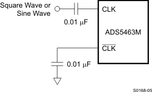 Figure 18. Single-Ended Clock
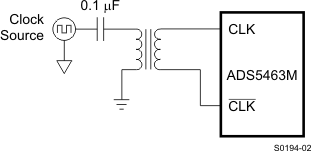 Figure 19. Differential Clock
For jitter-sensitive applications, the use of a differential clock has advantages (as with any other ADC) at the system level. The differential clock allows for common-mode noise rejection at the PCB level. With a differential clock, the signal-to-noise ratio of the ADC is better for high intermediate frequency applications because the board clock jitter is superior.
A differential clock also allows for the use of bigger clock amplitudes without exceeding the absolute maximum ratings. In the case of a sinusoidal clock, this results in higher slew rates and reduces the impact of clock noise on jitter. Figure 19 shows this approach. See Clocking High Speed Data Converters (SLYT075) for more details.
The common-mode voltage of the clock inputs is set internally to 2.4 V using internal 1-kΩ resistors. It is recommended to use ac coupling, but if this scheme is not possible due to, for instance, asynchronous clocking, the ADS5463 features good tolerance to clock common-mode variation. Additionally, the internal ADC core uses both edges of the clock for the conversion process. Ideally, a 50% duty-cycle clock signal should be provided.
8.1.3 Digital Outputs
The ADC provides 12 data outputs (D11 to D0, with D11 being the MSB and D0 the LSB), a data-ready signal (DRY), and an overrange indicator (OVR) that equals a logic high when the output reaches the full-scale limits. The output format is offset binary. It is recommended to use the DRY signal to capture the output data of the ADS5463. DRY is source-synchronous to the DATA/OVR bits and operates at the same frequency, creating a half-rate DDR interface that updates data on both the rising and falling edges of DRY. The ADS5463 digital outputs are LVDS-compatible. Due to the high data rates, care should be taken not to overload the digital outputs with too much capacitance, which shortens the data-valid timing window. The values given for timing were obtained with a measured 14-pF parasitic board capacitance to ground on each LVDS line (or 7-pF differential parasitic capacitance).
8.2 Typical Application
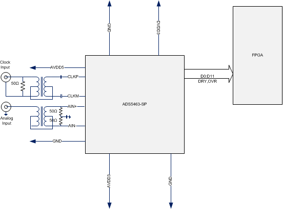 Figure 20. Application Diagram for ADS5463
8.2.1 Design Requirements
By using the simple drive circuit of Figure 2, Figure 15, or Figure 16, uniform performance can be obtained over a wide frequency range. The buffers present at the analog inputs of the device can help isolate the external drive source from the switching currents of the sampling circuit.
8.2.2 Detailed Design Procedure
For optimum performance, the analog inputs must be driven differentially. This architecture improves the common-mode noise immunity and even-order harmonic rejection.
8.2.3 Application Curve
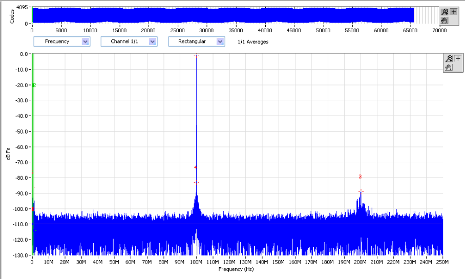 Figure 21. Typical Performance