SGLS378G March 2008 – October 2017 ADS5463-SP
PRODUCTION DATA.
- 1 Features
- 2 Applications
- 3 Description
- 4 Revision History
- 5 Pin Configuration and Functions
-
6 Specifications
- 6.1 Absolute Maximum Ratings
- 6.2 ESD Ratings
- 6.3 Recommended Operating Conditions
- 6.4 Thermal Information
- 6.5 Electrical Characteristics: ADS5463-RHA
- 6.6 Electrical Characteristics: ADS5463-RHA
- 6.7 Electrical Characteristics: ADS5463-RHA
- 6.8 Electrical Characteristics: ADS5463-SP
- 6.9 Electrical Characteristics: ADS5463-SP
- 6.10 Electrical Characteristics: ADS5463-SP
- 6.11 Timing Requirements
- 6.12 Typical Characteristics
- 7 Detailed Description
- 8 Application and Implementation
- 9 Power Supply Recommendations
- 10Layout
- 11Device and Documentation Support
- 12Mechanical, Packaging, and Orderable Information
Package Options
Mechanical Data (Package|Pins)
- HFG|84
Thermal pad, mechanical data (Package|Pins)
Orderable Information
6 Specifications
6.1 Absolute Maximum Ratings
over operating free-air temperature range (unless otherwise noted)(1)| MIN | MAX | UNIT | |||||
|---|---|---|---|---|---|---|---|
| Supply voltage | AVDD5 to GND | 6 | V | ||||
| AVDD3 to GND | 5 | ||||||
| DVDD3 to GND | 5 | ||||||
| AIN, AIN to GND(2) | Voltage difference between pin and ground |
AC signal | –0.3 | (AVDD5 + 0.3) | V | ||
| DC signal, TJ = 105°C | 0.4 | 4.4 | |||||
| DC signal, TJ = 125°C | 1.0 | 3.8 | |||||
| AIN to AIN(2) | Voltage difference between these pins |
AC signal | –5.2 | 5.2 | V | ||
| DC signal, TJ = 105°C | –4 | 4 | |||||
| DC signal, TJ = 125°C | –2.8 | 2.8 | |||||
| CLK, CLK to GND(2) | Voltage difference between pin and ground |
AC signal | –0.3 | (AVDD5 + 0.3) | V | ||
| DC signal, TJ = 105°C | 0.1 | 4.7 | |||||
| DC signal, TJ = 125°C | 1.1 | 3.7 | |||||
| CLK to CLK(2) | Voltage difference between these pins |
AC signal | –3.3 | 3.3 | V | ||
| DC signal, TJ = 105°C | –3.3 | 3.3 | |||||
| DC signal, TJ = 125°C | –2.6 | 2.6 | |||||
| Data output to GND(2) | LVDS digital outputs | –0.3 | (DVDD3 + 0.3) | V | |||
| Characterized case operating temperature, TC | –55 | 125 | °C | ||||
| Maximum junction temperature, TJ | 150 | °C | |||||
| Storage temperature, Tstg | –65 | 150 | °C | ||||
(1) Stresses beyond those listed under Absolute Maximum Ratings may cause permanent damage to the device. These are stress ratings only, which do not imply functional operation of the device at these or any other conditions beyond those indicated under Recommended Operating Conditions. Exposure to absolute-maximum-rated conditions for extended periods may affect device reliability.
(2) Valid when supplies are within recommended operating range.
6.2 ESD Ratings
| VALUE | UNIT | |||
|---|---|---|---|---|
| V(ESD) | Electrostatic discharge | Human-body model (HBM), per ANSI/ESDA/JEDEC JS-001(1) | ±3000 | V |
| Charged-device model (CDM), per JEDEC specification JESD22-C101(2) | ±1500 | |||
(1) JEDEC document JEP155 states that 500-V HBM allows safe manufacturing with a standard ESD control process.
(2) JEDEC document JEP157 states that 250-V CDM allows safe manufacturing with a standard ESD control process.
6.3 Recommended Operating Conditions
over operating free-air temperature range (unless otherwise noted)6.4 Thermal Information(2)
| THERMAL METRIC(1) | ADS5463-SP | UNIT | |
|---|---|---|---|
| HFG (CFP) | |||
| 84 PINS | |||
| RθJA | Junction-to-ambient thermal resistance | 17.9 | °C/W |
| RθJC(top) | Junction-to-case (top) thermal resistance | 3.1 | °C/W |
| RθJB | Junction-to-board thermal resistance | 6.1 | °C/W |
| ψJT | Junction-to-top characterization parameter | 1.4 | °C/W |
| ψJB | Junction-to-board characterization parameter | 5.6 | °C/W |
| RθJC(bot) | Junction-to-case (bottom) thermal resistance | 0.4 | °C/W |
(1) For more information about traditional and new thermal metrics, see the Semiconductor and IC Package Thermal Metrics application report, SPRA953.
(2) This CFP package has built-in vias that electrically and thermally connect the bottom of the die to a pad on the bottom of the package. To efficiently remove heat and provide a low-impedance ground path, a thermal land is required on the surface of the PCB directly underneath the body of the package. During normal surface mount flow solder operations, the heat pad on the underside of the package is soldered to this thermal land creating an efficient thermal path. Normally, the PCB thermal land has a number of thermal vias within it that provide a thermal path to internal copper areas (or to the opposite side of the PCB) that provide for more efficient heat removal. TI typically recommends an 11.9 mm2 board-mount thermal pad. This allows maximum area for thermal dissipation, while keeping leads away from the pad area to prevent solder bridging. A sufficient quantity of thermal/electrical vias must be included to keep the device within recommended operating conditions. This pad must be electrically at ground potential.
6.5 Electrical Characteristics: ADS5463-RHA
Typical values at TC = 25°C, full temperature range is TC,MIN = –55°C to TC,MAX = 125°C, sampling rate = 500 MSPS, 50% clock duty cycle, AVDD5 = 5 V, AVDD3 = 3.3 V, DVDD3 = 3.3 V, –1 dBFS differential input, and 3-VPP differential clock (unless otherwise noted)| PARAMETER | TEST CONDITIONS | MIN | TYP | MAX | UNIT | ||
|---|---|---|---|---|---|---|---|
| Resolution | 12 | Bits | |||||
| ANALOG INPUTS | |||||||
| Differential input range | 2.2 | VPP | |||||
| Input resistance (dc) | Each input to VCM | 500 | Ω | ||||
| Input capacitance | Each input to ground | 2.5 | pF | ||||
| Analog input bandwidth | 1000 | 2000 | MHz | ||||
| INTERNAL REFERENCE VOLTAGE | |||||||
| VREF | Reference voltage | Full temperature range | 2.38 | 2.4 | 2.42 | V | |
| DYNAMIC ACCURACY | |||||||
| No missing codes | Assured | ||||||
| DNL | Differential linearity error | fIN = 210 MHz | Full temperature range | –0.98 | ±0.95 | 1.2 | LSB |
| INL | Integral linearity error | fIN = 210 MHz | Full temperature range | –3.5 | ±1.5 | 3.5 | LSB |
| Offset error | Full temperature range | –0.5 | 0.5 | %FS | |||
| Offset temperature coefficient | 0.0009 | %FS/°C | |||||
| Gain error | Full temperature range | –5 | 5 | %FS | |||
| Gain temperature coefficient | –0.02 | %FS/°C | |||||
| POWER SUPPLY | |||||||
| IAVDD5 | 5 V analog supply current | VIN = full scale, fIN = 300 MHz, FS = 500 MSPS |
Full temperature range | 345 | mA | ||
| IAVDD3 | 3.3 V analog supply current | 148 | mA | ||||
| IDVDD3 | 3.3 V digital supply current(includes LVDS) | 88 | mA | ||||
| Power dissipation | 2.450 | W | |||||
6.6 Electrical Characteristics: ADS5463-RHA
Typical values at TC = 25°C, full temperature range is TC,MIN = –55°C to TC,MAX = 125°C, sampling rate = 500 MSPS, 50% clock duty cycle, AVDD5 = 5 V, AVDD3 = 3.3 V, DVDD3 = 3.3 V, –1 dBFS differential input, and 3-VPP differential clock (unless otherwise noted)| PARAMETER | TEST CONDITIONS | MIN | TYP | MAX | UNIT | ||
|---|---|---|---|---|---|---|---|
| DYNAMIC AC CHARACTERISTICS | |||||||
| SNR | Signal-to-noise ratio | fIN = 10 MHz | 65.4 | dBFS | |||
| fIN = 70 MHz | 65.3 | ||||||
| fIN = 100 MHz | TC = 25°C | 60.5 | 65.2 | ||||
| TC = TC,MAX | 60.5 | ||||||
| TC = TC,MIN | 60.5 | ||||||
| fIN = 210 MHz | TC = 25°C | 60 | 65 | ||||
| TC = TC,MAX | 60 | ||||||
| TC = TC,MIN | 60 | ||||||
| fIN = 300 MHz | TC = 25°C | 58 | 64.9 | ||||
| TC = TC,MAX | 58 | ||||||
| TC = TC,MIN | 58 | ||||||
| fIN = 450 MHz | 64.5 | ||||||
| fIN = 650 MHz | 63.7 | ||||||
| fIN = 900 MHz | 62.8 | ||||||
| fIN = 1.0 GHz | 62.2 | ||||||
| SFDR | Spurious free dynamic range | fIN = 10 MHz | 63.5 | dBc | |||
| fIN = 70 MHz | 64.2 | ||||||
| fIN = 100 MHz | TC = 25°C | 57.9 | 65 | ||||
| TC = TC,MAX | 57.9 | ||||||
| TC = TC,MIN | 57.9 | ||||||
| fIN = 210 MHz | TC = 25°C | 55.2 | 64 | ||||
| TC = TC,MAX | 55.2 | ||||||
| TC = TC,MIN | 55.2 | ||||||
| fIN = 300 MHz | TC = 25°C | 51.2 | 64 | ||||
| TC = TC,MAX | 51.2 | ||||||
| TC = TC,MIN | 51.2 | ||||||
| fIN = 450 MHz | 64 | ||||||
| fIN = 650 MHz | 61.6 | ||||||
| fIN = 900 MHz | 54.5 | ||||||
| fIN = 1.0 GHz | 51.6 | ||||||
| HD2 | Second harmonic | fIN = 10 MHz | 63.5 | dBc | |||
| fIN = 70 MHz | 64.2 | ||||||
| fIN = 100 MHz | TC = 25°C | 57.9 | 65.4 | ||||
| TC = TC,MAX | 57.9 | ||||||
| TC = TC,MIN | 57.9 | ||||||
| fIN = 210 MHz | TC = 25°C | 55.2 | 64.4 | ||||
| TC = TC,MAX | 55.2 | ||||||
| TC = TC,MIN | 55.2. | ||||||
| fIN = 300 MHz | TC = 25°C | 51.2 | 64.3 | ||||
| TC = TC,MAX | 51.2 | ||||||
| TC = TC,MIN | 51.2 | ||||||
| fIN = 450 MHz | 64.4 | ||||||
| fIN = 650 MHz | 67.1 | ||||||
| fIN = 900 MHz | 62.9 | ||||||
| fIN = 1.0 GHz | 58.6 | ||||||
| HD3 | Third harmonic | fIN = 10 MHz | 104 | dBc | |||
| fIN = 70 MHz | 104 | ||||||
| fIN = 100 MHz | TC = 25°C | 64 | 87 | ||||
| TC = TC,MAX | 64 | ||||||
| TC = TC,MIN | 64 | ||||||
| fIN = 210 MHz | TC = 25°C | 59 | 85 | ||||
| TC = TC,MAX | 59 | ||||||
| TC = TC,MIN | 59 | ||||||
| fIN = 300 MHz | TC = 25°C | 61.9 | 76 | ||||
| TC = TC,MAX | 61.9 | ||||||
| TC = TC,MIN | 61.9 | ||||||
| fIN = 450 MHz | 73.3 | ||||||
| fIN = 650 MHz | 61.6 | ||||||
| fIN = 900 MHz | 54.5 | ||||||
| fIN = 1.0 GHz | 51.6 | ||||||
6.7 Electrical Characteristics: ADS5463-RHA
Typical values at TC = 25°C, full temperature range is TC,MIN = –55°C to TC,MAX = 125°C, sampling rate = 500 MSPS, 50% clock duty cycle, AVDD5 = 5 V, AVDD3 = 3.3 V, DVDD3 = 3.3 V, –1 dBFS differential input, and 3-VPP differential clock (unless otherwise noted)| PARAMETER | TEST CONDITIONS | MIN | TYP | MAX | UNIT | ||
|---|---|---|---|---|---|---|---|
| DYNAMIC AC CHARACTERISTICS (CONT.) | |||||||
| SINAD | Signal-to-noise and distortion | fIN = 10 MHz | 61.9 | dBc | |||
| fIN = 70 MHz | 62.2 | ||||||
| fIN = 100 MHz | TC = 25°C | 55.9 | 62 | ||||
| TC = TC,MAX | 55.9 | ||||||
| TC = TC,MIN | 55.9 | ||||||
| fIN = 210 MHz | TC = 25°C | 53.8 | 62 | ||||
| TC = TC,MAX | 53.8 | ||||||
| TC = TC,MIN | 53.8 | ||||||
| fIN = 300 MHz | TC = 25°C | 50.2 | 61.9 | ||||
| TC = TC,MAX | 50.2 | ||||||
| TC = TC,MIN | 50.2 | ||||||
| fIN = 450 MHz | 61.6 | ||||||
| fIN = 650 MHz | 59.4 | ||||||
| fIN = 900 MHz | 54.3 | ||||||
| fIN = 1.0 GHz | 51.4 | ||||||
| Worst harmonic/spur (other than HD2 and HD3) | fIN = 10 MHz | 83.1 | dBc | ||||
| fIN = 70 MHz | 80.2 | ||||||
| fIN = 100 MHz | TC = 25°C | 68 | 81.8 | ||||
| TC = TC,MAX | 68 | ||||||
| TC = TC,MIN | 68 | ||||||
| fIN = 210 MHz | TC = 25°C | 62 | 77.5 | ||||
| TC = TC,MAX | 62 | ||||||
| TC = TC,MIN | 62 | ||||||
| fIN = 300 MHz | TC = 25°C | 62 | 78.2 | ||||
| TC = TC,MAX | 62 | ||||||
| TC = TC,MIN | 62 | ||||||
| fIN = 450 MHz | 80.6 | ||||||
| fIN = 650 MHz | 80 | ||||||
| fIN = 900 MHz | 79.4 | ||||||
| fIN = 1.0 GHz | 77.6 | ||||||
| THD | Total harmonic distortion | fIN = 10 MHz | 63.5 | dBc | |||
| fIN = 70 MHz | 64 | ||||||
| fIN = 100 MHz | TC = 25°C | 57.8 | 65.2 | ||||
| TC = TC,MAX | 57.8 | ||||||
| TC = TC,MIN | 57.8 | ||||||
| fIN = 210 MHz | TC = 25°C | 55 | 64.1 | ||||
| TC = TC,MAX | 55 | ||||||
| TC = TC,MIN | 55 | ||||||
| fIN = 300 MHz | TC = 25°C | 51 | 63.8 | ||||
| TC = TC,MAX | 51 | ||||||
| TC = TC,MIN | 51 | ||||||
| fIN = 450 MHz | 63.7 | ||||||
| fIN = 650 MHz | 60.5 | ||||||
| fIN = 900 MHz | 53.9 | ||||||
| fIN = 1.0 GHz | 50.8 | ||||||
| ENOB | Effective number of bits | fIN = 100 MHz | TC = 25°C | 9 | 10.1 | Bits | |
| TC = TC,MAX | 9 | ||||||
| TC = TC,MIN | 9 | ||||||
| fIN = 210 MHz | TC = 25°C | 8.65 | 10 | ||||
| TC = TC,MAX | 8.65 | ||||||
| TC = TC,MIN | 8.65 | ||||||
| fIN = 300 MHz | TC = 25°C | 8.05 | 9.9 | ||||
| TC = TC,MAX | 8.05 | ||||||
| TC = TC,MIN | 8.05 | ||||||
| RMS idle-channel noise | Inputs tied to common-mode | 0.7 | LSB | ||||
| LVDS DIGITAL OUTPUTS | |||||||
| VOD | Differential output voltage | 247 | 350 | 454 | mV | ||
| VOC | Common mode output voltage | 1.125 | 1.375 | V | |||
6.8 Electrical Characteristics: ADS5463-SP
Typical values at TC = 25°C, full temperature range is TC,MIN = –55°C to TC,MAX = 125°C, sampling rate = 500 MSPS, 50% clock duty cycle, AVDD5 = 5 V, AVDD3 = 3.3 V, DVDD3 = 3.3 V, –1 dBFS differential input, and 3-VPP differential clockover operating free-air temperature range (unless otherwise noted)| PARAMETER | TEST CONDITIONS | MIN | TYP | MAX | UNIT | ||
|---|---|---|---|---|---|---|---|
| Resolution | 12 | Bits | |||||
| ANALOG INPUTS | |||||||
| Differential input range | 2.2 | VPP | |||||
| Input resistance (dc) | Each input to VCM | 500 | Ω | ||||
| Input capacitance | Each input to ground | 2.5 | pF | ||||
| Analog input bandwidth | 1000 | 2000 | MHz | ||||
| INTERNAL REFERENCE VOLTAGE | |||||||
| VREF | Reference voltage | Full temperature range | 2.38 | 2.4 | 2.42 | V | |
| DYNAMIC ACCURACY | |||||||
| No missing codes | Assured | ||||||
| DNL | Differential linearity error | fIN = 210 MHz | Full temperature range | –0.98 | ±0.95 | 1.2 | LSB |
| INL | Integral linearity error | fIN = 210 MHz | Full temperature range | –2.9 | ±1.5 | 2.9 | LSB |
| Offset error | Full temperature range | –0.5 | 0.5 | %FS | |||
| Offset temperature coefficient | 0.0009 | %FS/°C | |||||
| Gain error | Full temperature range | –5 | 5 | %FS | |||
| Gain temperature coefficient | –0.02 | %FS/°C | |||||
| POWER SUPPLY | |||||||
| IAVDD5 | 5 V analog supply current | VIN = full scale, fIN = 300 MHz, FS = 500 MSPS |
Full temperature range | 335 | mA | ||
| IAVDD3 | 3.3 V analog supply current | 140 | mA | ||||
| IDVDD3 | 3.3 V digital supply current(includes LVDS) | 88 | mA | ||||
| Power dissipation | 2.425 | W | |||||
6.9 Electrical Characteristics: ADS5463-SP
Typical values at TC = 25°C, full temperature range is TC,MIN = –55°C to TC,MAX = 125°C, sampling rate = 500 MSPS, 50% clock duty cycle, AVDD5 = 5 V, AVDD3 = 3.3 V, DVDD3 = 3.3 V, –1 dBFS differential input, and 3-VPP differential clockover operating free-air temperature range (unless otherwise noted)| PARAMETER | TEST CONDITIONS | MIN | TYP | MAX | UNIT | ||
|---|---|---|---|---|---|---|---|
| DYNAMIC AC CHARACTERISTICS | |||||||
| SNR | Signal-to-noise ratio | fIN = 10 MHz | 65.4 | dBFS | |||
| fIN = 70 MHz | 65.3 | ||||||
| fIN = 100 MHz | TC = 25°C | 64.1 | 65.2 | ||||
| TC = TC,MAX | 62.7 | ||||||
| TC = TC,MIN | 63.5 | ||||||
| fIN = 210 MHz | TC = 25°C | 63.6 | 65 | ||||
| TC = TC,MAX | 62.4 | ||||||
| TC = TC,MIN | 63.2 | ||||||
| fIN = 300 MHz | TC = 25°C | 62.7 | 64.9 | ||||
| TC = TC,MAX | 61.3 | ||||||
| TC = TC,MIN | 61.9 | ||||||
| fIN = 450 MHz | 64.5 | ||||||
| fIN = 650 MHz | 63.7 | ||||||
| fIN = 900 MHz | 62.8 | ||||||
| fIN = 1.0 GHz | 62.2 | ||||||
| SFDR | Spurious free dynamic range | fIN = 10 MHz | 63.5 | dBc | |||
| fIN = 70 MHz | 64.2 | ||||||
| fIN = 100 MHz | TC = 25°C | 57.9 | 65 | ||||
| TC = TC,MAX | 58.8 | ||||||
| TC = TC,MIN | 58.6 | ||||||
| fIN = 210 MHz | TC = 25°C | 55.2 | 64.0 | ||||
| TC = TC,MAX | 56.6 | ||||||
| TC = TC,MIN | 56.9 | ||||||
| fIN = 300 MHz | TC = 25°C | 54.1 | 64 | ||||
| TC = TC,MAX | 51.3 | ||||||
| TC = TC,MIN | 56.2 | ||||||
| fIN = 450 MHz | 64 | ||||||
| fIN = 650 MHz | 61.6 | ||||||
| fIN = 900 MHz | 54.5 | ||||||
| fIN = 1.0 GHz | 51.6 | ||||||
| HD2 | Second harmonic | fIN = 10 MHz | 63.5 | dBc | |||
| fIN = 70 MHz | 64.2 | ||||||
| fIN = 100 MHz | TC = 25°C | 57.9 | 65.4 | ||||
| TC = TC,MAX | 58.8 | ||||||
| TC = TC,MIN | 58.6 | ||||||
| fIN = 210 MHz | TC = 25°C | 55.2 | 64.4 | ||||
| TC = TC,MAX | 56.6 | ||||||
| TC = TC,MIN | 56.9 | ||||||
| fIN = 300 MHz | TC = 25°C | 54.1 | 64.3 | ||||
| TC = TC,MAX | 51.3 | ||||||
| TC = TC,MIN | 56.2 | ||||||
| fIN = 450 MHz | 64.4 | ||||||
| fIN = 650 MHz | 67.1 | ||||||
| fIN = 900 MHz | 62.9 | ||||||
| fIN = 1.0 GHz | 58.6 | ||||||
| HD3 | Third harmonic | fIN = 10 MHz | 104 | dBc | |||
| fIN = 70 MHz | 104 | ||||||
| fIN = 100 MHz | TC = 25°C | 69 | 87 | ||||
| TC = TC,MAX | 68.5 | ||||||
| TC = TC,MIN | 65.6 | ||||||
| fIN = 210 MHz | TC = 25°C | 66.7 | 85 | ||||
| TC = TC,MAX | 65.3 | ||||||
| TC = TC,MIN | 64.1 | ||||||
| fIN = 300 MHz | TC = 25°C | 70.1 | 76 | ||||
| TC = TC,MAX | 61.9 | ||||||
| TC = TC,MIN | 64.8 | ||||||
| fIN = 450 MHz | 73.3 | ||||||
| fIN = 650 MHz | 61.6 | ||||||
| fIN = 900 MHz | 54.5 | ||||||
| fIN = 1.0 GHz | 51.6 | ||||||
6.10 Electrical Characteristics: ADS5463-SP
Typical values at TC = 25°C, full temperature range is TC,MIN = –55°C to TC,MAX = 125°C, sampling rate = 500 MSPS, 50% clock duty cycle, AVDD5 = 5 V, AVDD3 = 3.3 V, DVDD3 = 3.3 V, –1 dBFS differential input, and 3-VPP differential clockover operating free-air temperature range (unless otherwise noted)| PARAMETER | TEST CONDITIONS | MIN | TYP | MAX | UNIT | ||
|---|---|---|---|---|---|---|---|
| DYNAMIC AC CHARACTERISTICS (CONT.) | |||||||
| SINAD | Signal-to-noise and distortion | fIN = 10 MHz | 61.9 | dBc | |||
| fIN = 70 MHz | 62.2 | ||||||
| fIN = 100 MHz | TC = 25°C | 58 | 62 | ||||
| TC = TC,MAX | 58 | ||||||
| TC = TC,MIN | 58.4 | ||||||
| fIN = 210 MHz | TC = 25°C | 55.8 | 62 | ||||
| TC = TC,MAX | 56.2 | ||||||
| TC = TC,MIN | 56.7 | ||||||
| fIN = 300 MHz | TC = 25°C | 54.9 | 61.9 | ||||
| TC = TC,MAX | 52.2 | ||||||
| TC = TC,MIN | 56.1 | ||||||
| fIN = 450 MHz | 61.6 | ||||||
| fIN = 650 MHz | 59.4 | ||||||
| fIN = 900 MHz | 54.3 | ||||||
| fIN = 1.0 GHz | 51.4 | ||||||
| Worst harmonic/spur (other than HD2 and HD3) | fIN = 10 MHz | 83.1 | dBc | ||||
| fIN = 70 MHz | 80.2 | ||||||
| fIN = 100 MHz | TC = 25°C | 72.2 | 81.8 | ||||
| TC = TC,MAX | 70.6 | ||||||
| TC = TC,MIN | 72.6 | ||||||
| fIN = 210 MHz | TC = 25°C | 70.6 | 77.5 | ||||
| TC = TC,MAX | 67.1 | ||||||
| TC = TC,MIN | 66.5 | ||||||
| fIN = 300 MHz | TC = 25°C | 69.3 | 78.2 | ||||
| TC = TC,MAX | 66.3 | ||||||
| TC = TC,MIN | 66.3 | ||||||
| fIN = 450 MHz | 80.6 | ||||||
| fIN = 650 MHz | 80 | ||||||
| fIN = 900 MHz | 79.4 | ||||||
| fIN = 1.0 GHz | 77.6 | ||||||
| THD | Total harmonic distortion | fIN = 10 MHz | 63.5 | dBc | |||
| fIN = 70 MHz | 64 | ||||||
| fIN = 100 MHz | TC = 25°C | 57.8 | 65.2 | ||||
| TC = TC,MAX | 58.3 | ||||||
| TC = TC,MIN | 58.1 | ||||||
| fIN = 210 MHz | TC = 25°C | 55 | 64.1 | ||||
| TC = TC,MAX | 55.9 | ||||||
| TC = TC,MIN | 56.2 | ||||||
| fIN = 300 MHz | TC = 25°C | 53.9 | 63.8 | ||||
| TC = TC,MAX | 51 | ||||||
| TC = TC,MIN | 55.6 | ||||||
| fIN = 450 MHz | 63.7 | ||||||
| fIN = 650 MHz | 60.5 | ||||||
| fIN = 900 MHz | 53.9 | ||||||
| fIN = 1.0 GHz | 50.8 | ||||||
| ENOB | Effective number of bits | fIN = 100 MHz | TC = 25°C | 9.3 | 10.1 | Bits | |
| TC = TC,MAX | 9.3 | ||||||
| TC = TC,MIN | 9.4 | ||||||
| fIN = 210 MHz | TC = 25°C | 8.9 | 10 | ||||
| TC = TC,MAX | 9 | ||||||
| TC = TC,MIN | 9.1 | ||||||
| fIN = 300 MHz | TC = 25°C | 8.8 | 9.9 | ||||
| TC = TC,MAX | 8.3 | ||||||
| TC = TC,MIN | 9 | ||||||
| RMS idle-channel noise | Inputs tied to common-mode | 0.7 | LSB | ||||
| LVDS DIGITAL OUTPUTS | |||||||
| VOD | Differential output voltage | 247 | 350 | 454 | mV | ||
| VOC | Common mode output voltage | 1.125 | 1.375 | V | |||
6.11 Timing Requirements
Typical values at TC = 25°C, full temperature range is TC,MIN = –55°C to TC,MAX = 125°C, sampling rate = 500 MSPS, 50% clock duty cycle, AVDD5 = 5 V, AVDD3 = 3.3 V, DVDD3 = 3.3 V, and 3 VPP differential clock (unless otherwise noted)(1).| MIN | NOM | MAX | UNIT | |||
|---|---|---|---|---|---|---|
| ta | Aperture delay | 200 | ps | |||
| Aperture jitter, rms | 160 | fs | ||||
| Latency | 3.5 | cycles | ||||
| tCLK | Clock period | 2 | 50 | ns | ||
| tCLKH | Clock pulse duration, high | 1 | ns | |||
| tCLKL | Clock pulse duration, low | 1 | ns | |||
| tDRY | CLK to DRY delay(2) | Zero crossing | 750 | 1500 | 2500 | ps |
| tDATA | CLK to DATA/OVR delay(2) | Zero crossing | 650 | 1500 | 3100 | ps |
| tSKEW | DATA to DRY skew | tDATA–tDRY | –700 | 0 | 700 | ps |
| tRISE | DRY/DATA/OVR rise time | 500 | ps | |||
| tFALL | DRY/DATA/OVR fall time | 500 | ps | |||
(1) Timing parameters are assured by design or characterization, but not production tested. < 10-pF load on each output pin.
(2) DRY, DATA and OVR are updated on the falling edge of CLK. The latency must be added to tDATA to determine the overall propagation delay.
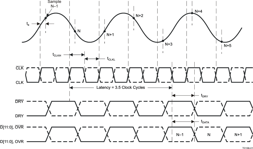 Figure 1. Timing Diagram
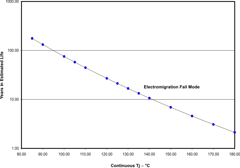 Figure 2. ADS5463 Estimated Life at Elevated Temperature Electromigration Fail Mode
6.12 Typical Characteristics
Typical plots at TA = 25°C, sampling rate = 500 MSPS, 50% clock duty cycle, AVDD5 = 5 V, AVDD3 = 3.3 V, DVDD3 = 3.3 V, and 3 VPP differential clock, (unless otherwise noted)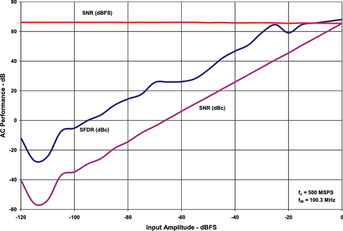 Figure 3. AC Performance vs Input Amplitude (100-MHz Input Signal)
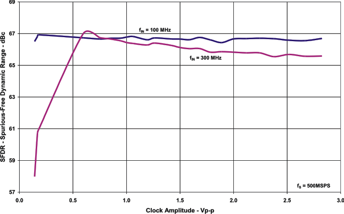 Figure 5. SFDR vs Clock Level
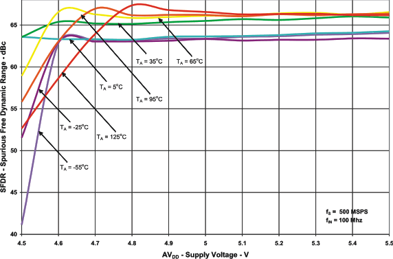 Figure 7. SFDR vs AVDD5 Across Temperature
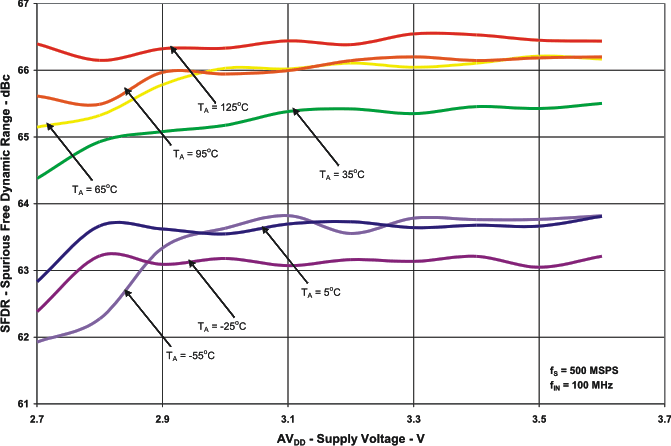 Figure 9. SFDR vs AVDD3 Across Temperature
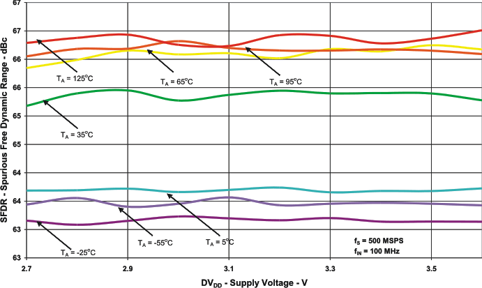 Figure 11. SFDR vs DVDD3 Across Temperature
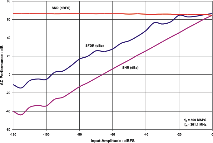 Figure 4. AC Performance vs Input Amplitude (300-MHz Input Signal)
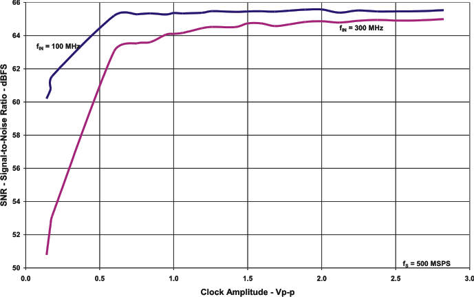 Figure 6. SNR vs Clock Level
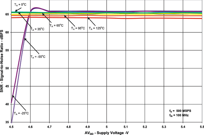 Figure 8. SNR vs AVDD5 Across Temperature
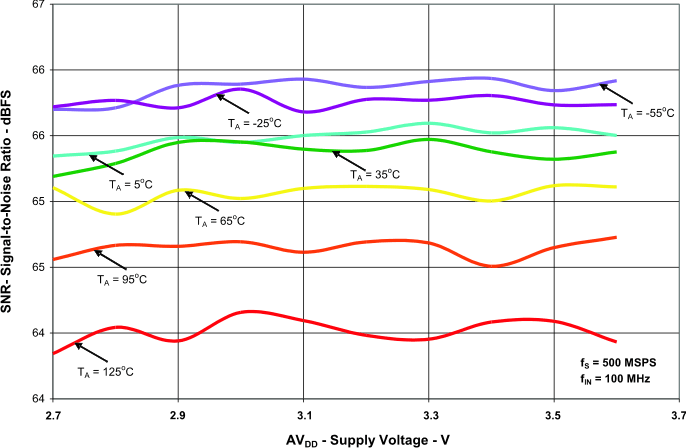 Figure 10. SNR vs AVDD3 Across Temperature
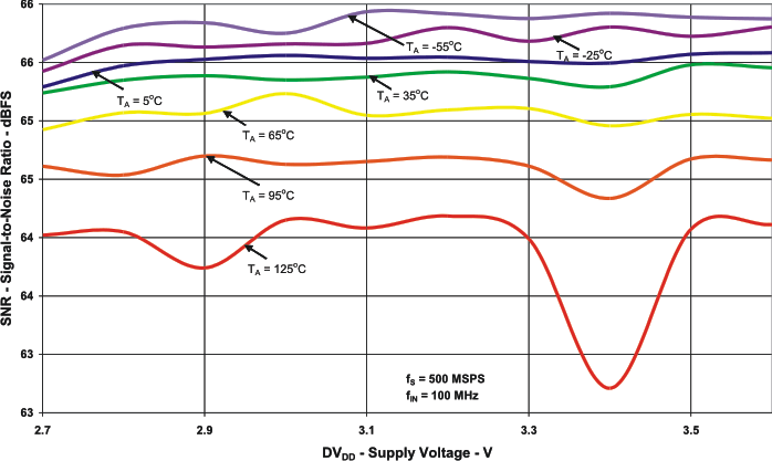 Figure 12. SNR vs DVDD3 Across Temperature
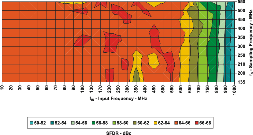 Figure 13. SFDR vs Input Frequency and Sampling Frequency
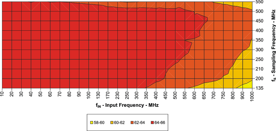 Figure 14. SNR vs Input Frequency and Sampling Frequency