SLAS525D July 2007 – December 2017 ADS5474
PRODUCTION DATA.
- 1 Features
- 2 Applications
- 3 Description
- 4 Revision History
- 5 Pin Configuration and Functions
- 6 Specifications
- 7 Detailed Description
- 8 Application and Implementation
- 9 Power Supply Recommendations
- 10Layout
- 11Device and Documentation Support
- 12Mechanical, Packaging, and Orderable Information
Package Options
Mechanical Data (Package|Pins)
- PFP|80
Thermal pad, mechanical data (Package|Pins)
- PFP|80
Orderable Information
9 Power Supply Recommendations
9.1 Power Supplies
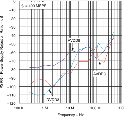
The ADS5474 device uses three power supplies. For the analog portion of the design, a 5-V and 3.3-V supply (AVDD5 and AVDD3) are used, while the digital portion uses a 3.3-V supply (DVDD3). Using low-noise power supplies with adequate decoupling is recommended. Linear supplies are preferred to switched supplies, as switched supplies tend to generate more noise components that can be coupled to the ADS5474 device. However, the PSRR value and the plot shown in Figure 46 were obtained without bulk supply decoupling capacitors. When bulk (0.1-μF) decoupling capacitors are used, the board-level PSRR is much higher than the stated value for the ADC. The user may be able to supply power to the device with a less-than-ideal supply and still achieve good performance. It is not possible to make a single recommendation for every type of supply and level of decoupling for all systems. If the noise characteristics of the available supplies are understood, a study of the PSRR data for the ADS5474 device may provide the user with enough information to select noisy supplies if the performance is still acceptable within the frequency range of interest. The power consumption of the ADS5474 device does not change substantially over clock rate or input frequency as a result of the architecture and process. The DVDD3 PSRR is superior to both the AVDD5 and AVDD3, and therefore was not graphed.
Because there are two diodes connected in reverse between AVDD3 and DVDD3 internally, a power-up sequence is recommended. When there is a delay in power up between these two supplies, the one that lags could have current sinking through an internal diode before it powers up. The sink current can be large or small depending on the impedance of the external supply and could damage the device or affect the supply source. The best power up sequence is one of the following options (regardless of when AVDD5 powers up):
1) Power up both AVDD3 and DVDD3 at the same time (best scenario), OR
2) Keep the voltage difference less than 0.8 V between AVDD3 and DVDD3 during the power up (0.8 V is not a hard specification - a smaller delta between supplies is safer).
If the above sequences are not practical then the sink current from the supply must be controlled or protection added externally. The max transient current (on the order of μsec) for DVDD3 or AVDD3 pin is 500 mA to avoid potential damage to the device or reduce its lifetime.
Values for analog and clock input given in the Absolute Maximum Ratings are valid when the supplies are on. When the power supplies are off and the clock or analog inputs are still alive, the input voltage and current must be limited to avoid device damage. If the ADC supplies are off, the max, min continuous DC voltage is ±0.95 V and max DC current is 20 mA for each input pin (clock or analog), relative to ground.
 Figure 46. PSRR vs Supply Injected Frequency