SLASE67A January 2015 – August 2019 ADS54J54
PRODUCTION DATA.
- 1 Features
- 2 Applications
- 3 Description
- 4 Revision History
- 5 Pin Configuration and Functions
-
6 Specifications
- 6.1 Absolute Maximum Ratings
- 6.2 ESD Ratings
- 6.3 Recommended Operating Conditions
- 6.4 Thermal Information
- 6.5 Electrical Characteristics
- 6.6 Electrical Characteristics: 250 MSPS Output, 2x Decimation Filter
- 6.7 Electrical Characteristics: 500 MSPS Output
- 6.8 Electrical Characteristics: Sample Clock Timing Characteristics
- 6.9 Electrical Characteristics: Digital Outputs
- 6.10 Timing Requirements
- 6.11 Reset Timing
- 6.12 Typical Characteristics
-
7 Detailed Description
- 7.1 Overview
- 7.2 Functional Block Diagram
- 7.3
Feature Description
- 7.3.1 Decimation by 2 (250 MSPS Output)
- 7.3.2 Over-Range Indication
- 7.3.3 JESD204B Interface
- 7.3.4 SYSREF Clocking Schemes
- 7.3.5 Split-Mode Operation
- 7.3.6 Eye Diagram Information
- 7.3.7 Analog Inputs
- 7.3.8 Clock Inputs
- 7.3.9 Input Clock Divider
- 7.3.10 Power-Down Control
- 7.3.11 Device Configuration
- 7.3.12 JESD204B Interface Initialization Sequence
- 7.3.13 Device and Register Initialization
- 7.4 Device Functional Modes
- 7.5 Programming
- 7.6
Register Maps
- 7.6.1
Register Descriptions
- 7.6.1.1 Register Address 0
- 7.6.1.2 Register Address 1
- 7.6.1.3 Register Address 3
- 7.6.1.4 Register Address 4
- 7.6.1.5 Register Address 5
- 7.6.1.6 Register Address 6
- 7.6.1.7 Register Address 7
- 7.6.1.8 Register Address 8
- 7.6.1.9 Register Address 12
- 7.6.1.10 Register Address 13
- 7.6.1.11 Register Address 14
- 7.6.1.12 Register Address 15
- 7.6.1.13 Register Address 16
- 7.6.1.14 Register Address 19
- 7.6.1.15 Register Address 22
- 7.6.1.16 Register Address 23
- 7.6.1.17 Register Address 26
- 7.6.1.18 Register Address 29
- 7.6.1.19 Register Address 30
- 7.6.1.20 Register Address 31
- 7.6.1.21 Register Address 32
- 7.6.1.22 Register Address 33
- 7.6.1.23 Register Address 99
- 7.6.1.24 Register Address 100
- 7.6.1.25 Register Address 103
- 7.6.1.26 Register Address 104
- 7.6.1.27 Register Address 107
- 7.6.1.28 Register Address 108
- 7.6.1
Register Descriptions
- 8 Application and Implementation
- 9 Power Supply Recommendations
- 10Layout
- 11Device and Documentation Support
- 12Mechanical, Packaging, and Orderable Information
Package Options
Mechanical Data (Package|Pins)
- RGC|64
Thermal pad, mechanical data (Package|Pins)
- RGC|64
Orderable Information
6.12 Typical Characteristics
Typical values at TA = 25°C, full temperature range is TMIN = –40°C to TMAX = 85°C, Device clock frequency = 500 MHz, Output sample data rate = 5Gbps, 50% Device clock duty cycle, AVDD33 = 3.3 V, AVDD18 = 1.9 V, AVDDC = 1.8 V, IOVDD = 1.8 V, PLLVDD = 1.8 V, DVDD = 1.8 V, –1 dBFS differential input, unless otherwise noted, FFT sample size = 32768.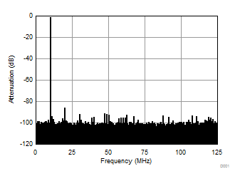
| Fin = 10 MHz | 1-lane 2x decimation | Ain = –1 dBFS |
| SNR = 65.29 dBFS | SFDR = 84.72 dBc |
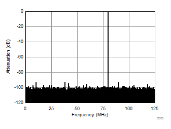
| Fin = 170 MHz | 1-lane 2x decimation | Ain = –1 dBFS |
| SNR = 65.34 dBFS | SFDR = 91.62 dBc |
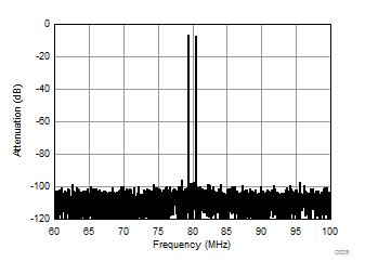
| Fin = 230 MHz | 1-lane 2x decimation | Ain = –1 dBFS |
| SNR = 65.16 dBFS | SFDR = 76.83 dBc |
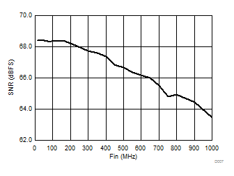
| 1-lane 2x decimation | Ain = –1 dBFS |
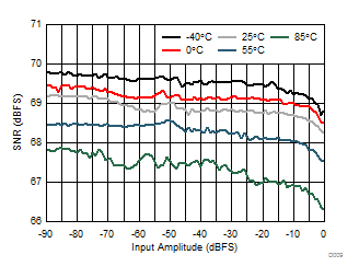
| 1-lane 2x decimation | Fin = 170 MHz |
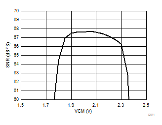
| 1-lane 2x decimation | Fin = 170 MHz |
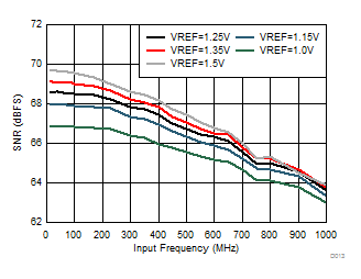
| 1-lane 2x decimation | Ain = –1 dBFS |
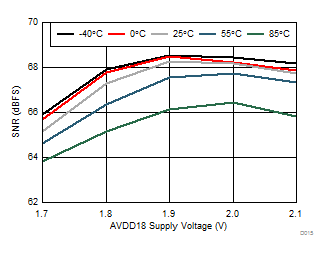
| 1-lane 2x decimation | Ain = –1 dBFS | Fin = 170 MHz |
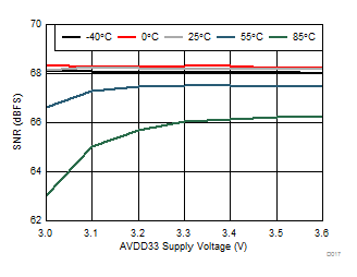
| 1-lane 2x decimation | Ain = –1 dBFS | Fin = 170 MHz |
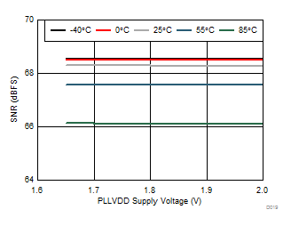
| 1-lane 2x decimation | Ain = –1 dBFS | Fin = 170 MHz |
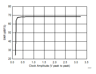
| 1-lane 2x decimation | Ain = –1 dBFS | Fin = 170 MHz |
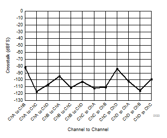
| 1-lane 2x decimation | Ain = –1 dBFS | Fin = 170 MHz |
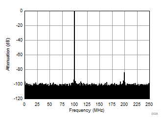
| 2-lane no decimation | Ain = –1 dBFS | Fin = 100 MHz |
| SNR = 65.41 dBFS | SFDR = 83.25 dBc |
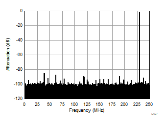
| 2-lane no decimation | Ain = –1 dBFS | Fin = 230 MHz |
| SNR = 64.91 dBFS | SFDR = 83.29 dBc |
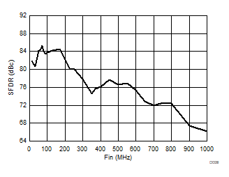
| 2-lane no decimation | Ain = –1 dBFS |
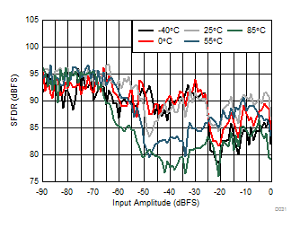
| 2-lane no decimation | Fin = 170 MHz | |
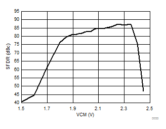
| 2-lane no decimation | Fin = 170 MHz | |
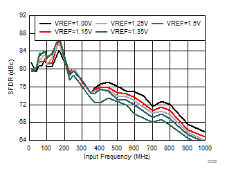
| 2-lane no decimation | Ain = –1 dBFS | |
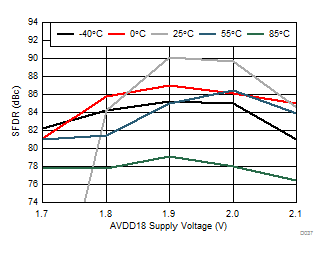
| 2-lane no decimation | Ain = –1 dBFS | Fin = 170 MHz |
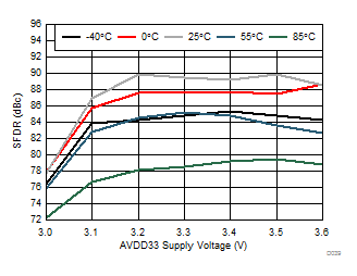
| 2-lane no decimation | Ain = –1 dBFS | Fin = 170 MHz |
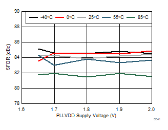
| 2-lane no decimation | Ain = –1 dBFS | Fin = 170 MHz |
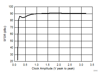
| 2-lane no decimation | Ain = –1 dBFS | Fin = 170 MHz |
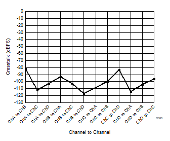
| 2-lane no decimation | Ain = –1 dBFS | Fin = 170 MHz | ||
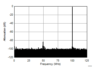
| Fin = 100 MHz | 1-lane 2x decimation | Ain = –1 dBFS |
| SNR = 65.40 dBFS | SFDR = 82.50 dBc |
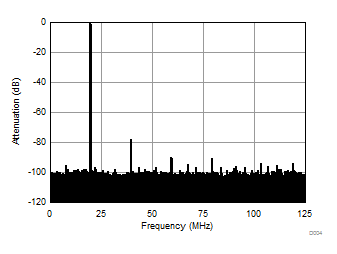
| Fin = 230 MHz | 1-lane 2x decimation | Ain = –1 dBFS |
| SNR = 65.16 dBFS | SFDR = 76.83 dBc |
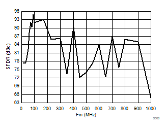
| 1-lane 2x decimation | Ain = –1 dBFS | |
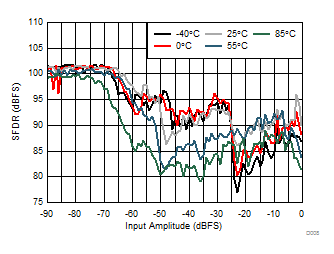
| 1-lane 2x decimation | Fin = 170 MHz |
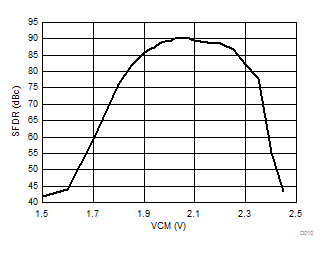
| 1-lane 2x decimation | Fin = 170 MHz |
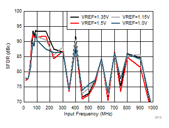
| 1-lane 2x decimation | Ain = –1 dBFS |
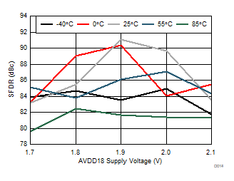
| 1-lane 2x decimation | Ain = –1 dBFS | Fin = 170 MHz |
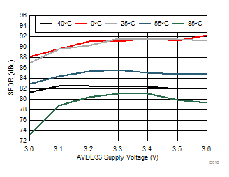
| 1-lane 2x decimation | Ain = –1 dBFS | Fin = 170 MHz |
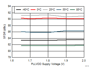
| 1-lane 2x decimation | Ain = –1 dBFS | Fin = 170 MHz |
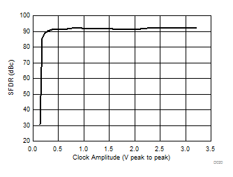
| 1-lane 2x decimation | Ain = –1 dBFS | Fin = 170 MHz |
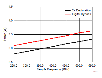
| AVDD18 = 1.9 V | AVDD33 = 3.3 V | Other supplies = 1.8 V |
| Ain = –1 dBFS | Fin = 170 MHz |
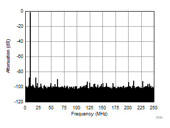
| 2-lane no decimation | Ain = –1 dBFS | Fin = 10 MHz |
| SNR = 65.27 dBFS | SFDR = 86.63 dBc |
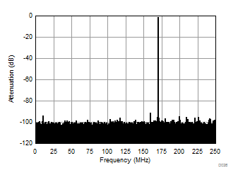
| 2-lane no decimation | Ain = –1 dBFS | Fin = 170 MHz |
| SNR = 65.26 dBFS | SFDR = 90.42 dBc |
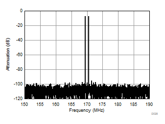
| 2-lane no decimation | Ain = –1 dBFS | |
| Fin = 170 MHz | ||
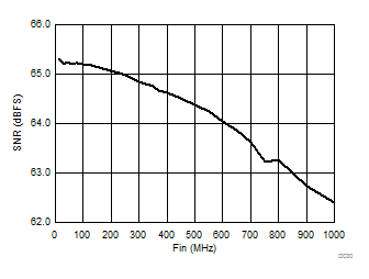
| 2-lane no decimation | Ain = –1 dBFS |
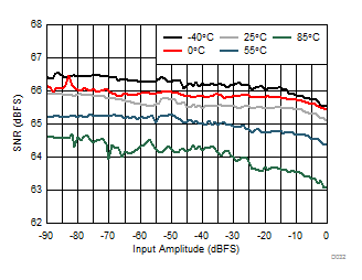
| 2-lane no decimation | Fin = 170 MHz | |
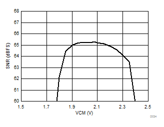
| 2-lane no decimation | Fin = 170 MHz | |
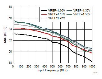
| 2-lane no decimation | Ain = –1 dBFS | |
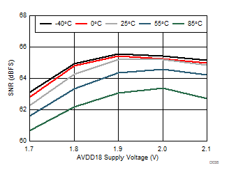
| 2-lane no decimation | Ain = –1 dBFS | Fin = 170 MHz |
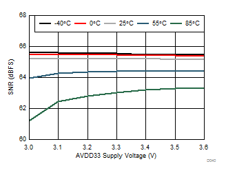
| 2-lane no decimation | Ain = –1 dBFS | Fin = 170 MHz |
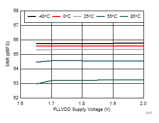
| 2-lane no decimation | Ain = –1 dBFS | Fin = 170 MHz |
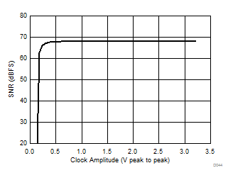
| 2-lane no decimation | Ain = –1 dBFS | Fin = 170 MHz |
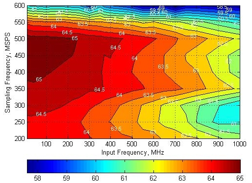
2lane no decimation
Figure 50. SNR Contour Plot 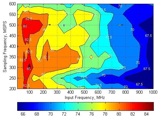
2lane no decimation
Figure 51. SFDR Contour Plot 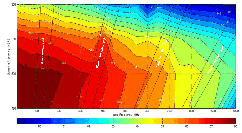
1lane 2x decimation
Figure 52. SNR Contour Plot 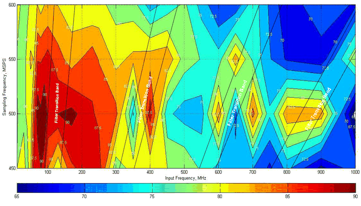
1lane 2x decimation
Figure 53. SFDR Contour Plot