SLAS918B December 2012 – April 2022 ADS54T01
PRODUCTION DATA
- 1 Features
- 2 Applications
- 3 Description
- 4 Revision History
- 5 Device Comparison
- 6 Pin Configuration and Functions
- 7 Specifications
-
8 Detailed Description
- 8.1 Overview
- 8.2 Functional Block Diagram
- 8.3
Feature Description
- 8.3.1 Test Pattern Output
- 8.3.2 Clock Inputs
- 8.3.3 SNR and Clock Jitter
- 8.3.4 Analog Inputs
- 8.3.5 Over-Range Indication
- 8.3.6 Interleaving Correction
- 8.3.7 High-Resolution Output Data
- 8.3.8 Low-Resolution Output Data
- 8.3.9 Full Speed – 7 Bit
- 8.3.10 Decimated Low-Resolution Output Data
- 8.3.11 Multi Device Synchronization
- 8.4 Device Functional Modes
- 8.5 Programming
- 8.6 Register Maps
- 9 Power Supply Recommendations
- 10Device and Documentation Support
- 11Mechanical, Packaging, and Orderable Information
Package Options
Mechanical Data (Package|Pins)
- ZAY|196
Thermal pad, mechanical data (Package|Pins)
Orderable Information
3 Description
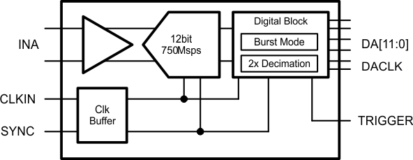
The ADS54T01 is a high linearity, single channel, 12-bit, 750-Msps analog-to-digital converter (ADC) easing front end filter design for wide bandwidth receivers. The analog input buffer isolates the internal switching of the on-chip track-and-hold from disturbing the signal source as well as providing a high-impedance input.
Two output modes are available for the output data—the data can be decimated by two or the data can be output in burst mode. The burst mode output is designed specifically for DPD feedback applications where high-resolution output data is available for a short period of time. Designed for high SFDR, the ADC has low-noise performance and outstanding spurious-free dynamic range over a large input-frequency range. The device is available in a 196-pin NFBGA package and is specified over the full industrial temperature range (–40°C to 85°C).
| PART NUMBER | PACKAGE(1) | BODY SIZE (NOM) |
|---|---|---|
| ADS54T01 | NFBGA (196) | 12.00 mm × 12.00 mm |
 Functional Block Diagram