SBAS682D November   2014  – December 2015 ADS7044

PRODUCTION DATA.  

  1. Features
  2. Applications
  3. Description
  4. Revision History
  5. Pin Configuration and Functions
  6. Specifications
    1. 6.1 Absolute Maximum Ratings
    2. 6.2 ESD Ratings
    3. 6.3 Recommended Operating Conditions
    4. 6.4 Thermal Information
    5. 6.5 Electrical Characteristics
    6. 6.6 Timing Characteristics
    7. 6.7 Typical Characteristics
  7. Parameter Measurement Information
    1. 7.1 Digital Voltage Levels
  8. Detailed Description
    1. 8.1 Overview
    2. 8.2 Functional Block Diagram
    3. 8.3 Feature Description
      1. 8.3.1 Reference
      2. 8.3.2 Analog Input
      3. 8.3.3 ADC Transfer Function
      4. 8.3.4 Serial Interface
    4. 8.4 Device Functional Modes
      1. 8.4.1 Offset Calibration
        1. 8.4.1.1 Offset Calibration on Power-Up
        2. 8.4.1.2 Offset Calibration During Normal Operation
  9. Application and Implementation
    1. 9.1 Application Information
    2. 9.2 Typical Applications
      1. 9.2.1 Single-Supply DAQ with the ADS7044
        1. 9.2.1.1 Design Requirements
        2. 9.2.1.2 Detailed Design Procedure
          1. 9.2.1.2.1 Antialiasing Filter
          2. 9.2.1.2.2 Input Amplifier Selection
          3. 9.2.1.2.3 Reference Circuit
        3. 9.2.1.3 Application Curve
      2. 9.2.2 Ultra-Low Power and Ultra-Small, High CMRR DAQ Circuit with the ADS7044
        1. 9.2.2.1 Design Requirements
        2. 9.2.2.2 Detailed Design Procedure
        3. 9.2.2.3 Application Curves
  10. 10Power-Supply Recommendations
    1. 10.1 AVDD and DVDD Supply Recommendations
    2. 10.2 Estimating Digital Power Consumption
    3. 10.3 Optimizing Power Consumed by the Device
  11. 11Layout
    1. 11.1 Layout Guidelines
    2. 11.2 Layout Example
  12. 12Device and Documentation Support
    1. 12.1 Documentation Support
      1. 12.1.1 Related Documentation
    2. 12.2 Community Resources
    3. 12.3 Trademarks
    4. 12.4 Electrostatic Discharge Caution
    5. 12.5 Glossary
  13. 13Mechanical, Packaging, and Orderable Information

Package Options

Refer to the PDF data sheet for device specific package drawings

Mechanical Data (Package|Pins)
  • DCU|8
  • RUG|8
Thermal pad, mechanical data (Package|Pins)
Orderable Information

5 Pin Configuration and Functions

RUG Package
8-Pin X2QFN
Top View
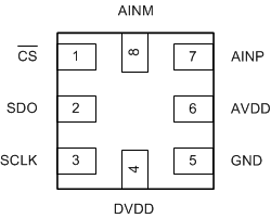
ADS7044 po_rug8_bas608.gif
DCU Package
8-Pin Leaded VSSOP
Top View
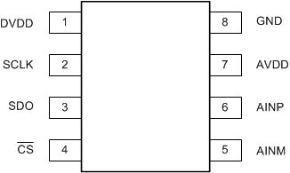
ADS7044 po_dcu8_bas608.gif

Pin Functions

PIN I/O DESCRIPTION
NAME NO.
RUG DCU
AINM 8 5 Analog input Analog signal input, negative
AINP 7 6 Analog input Analog signal input, positive
AVDD 6 7 Supply Analog power-supply input, also provides the reference voltage to the ADC
CS 1 4 Digital input Chip-select signal, active low
DVDD 4 1 Supply Digital I/O supply voltage
GND 5 8 Supply Ground for power supply, all analog and digital signals are referred to this pin
SCLK 3 2 Digital input Serial clock
SDO 2 3 Digital output Serial data out