SBAS785 December 2016 ADS7046
PRODUCTION DATA.
- 1 Features
- 2 Applications
- 3 Description
- 4 Revision History
- 5 Pin Configuration and Functions
- 6 Specifications
- 7 Parameter Measurement Information
- 8 Detailed Description
- 9 Application and Implementation
- 10Power Supply Recommendations
- 11Layout
- 12Device and Documentation Support
- 13Mechanical, Packaging, and Orderable Information
Package Options
Mechanical Data (Package|Pins)
- RUG|8
Thermal pad, mechanical data (Package|Pins)
- RUG|8
Orderable Information
8 Detailed Description
8.1 Overview
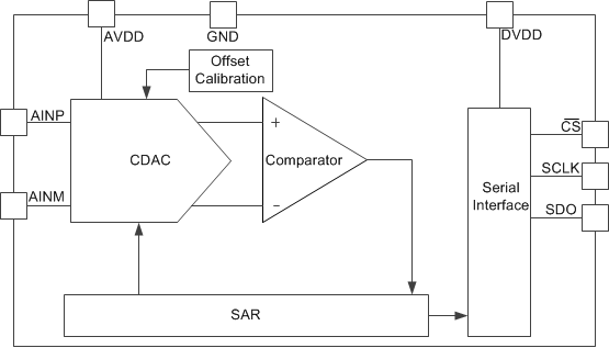
The ADS7046 device belongs to a family of pin-to-pin compatible, high-speed, low-power, single-channel successive-approximation register (SAR) type analog-to-digital converters (ADCs). The device family includes multiple resolutions, throughputs, and analog input variants (see Table 1 for a list of devices).
The ADS7046 is a 12-bit, 3-MSPS SAR ADC that supports a single-ended input in the range of 0 V to AVDD, for AVDD in the range of 2.35 V to 3.6 V (see the Analog Input section for details on the analog input pins).
The internal offset calibration feature (see the OFFCAL State section) maintains excellent offset specifications over the entire AVDD and temperature operating range.
The device supports an SPI-compatible serial interface that is controlled by the CS and SCLK signals. The input signal is sampled with the CS falling edge and SCLK is used for both, conversion and serial data output (see the Device Functional Modes section, Timing Requirements table, and Switching Characteristics table).
The device supports a wide digital supply range (1.65 V to 3.6 V), enabling direct interfacing to a variety of host controllers. The ADS7046 complies with the JESD8-7A standard (see the Digital Voltage Levels section) for a normal DVDD range (1.65 V to 1.95 V).
The ADS7046 is available in an 8-pin, small, X2QFN package (see the Mechanical, Packaging, and Orderable Information section for more details) and is specified over the extended industrial temperature range (–40°C to +125°C).
The small form-factor and extremely-low power consumption make this device suitable for space-constrained and battery-powered applications that require high-speed, high-resolution data acquisition (see the Application Information section).
8.2 Functional Block Diagram

8.3 Feature Description
8.3.1 Product Family
The devices listed in Table 1 are all part of the same pin-to-pin compatible, high-speed, low-power, single-channel SAR ADC family. This device family includes multiple different ADC resolutions, throughputs, and analog input types to allow for greater flexibility in the end system. Devices in the same package are pin-compatible to offer a scalable family of devices for varying levels of end-system performance. The ADCs with device numbers ending in -Q1 are also AEC-Q100 qualified for automotive applications.
Table 1. Device Family Comparison
| DEVICE NUMBER | RESOLUTION (Bits) | THROUGHPUT (MSPS) | INPUT TYPE | PACKAGES(1) |
|---|---|---|---|---|
| ADS7040 | 8 | 1 | Single-ended | X2QFN (8): 1.5 mm × 1.5 mm VSSOP (8): 2.0 mm × 3.1 mm |
| ADS7041 | 10 | 1 | Single-ended | X2QFN (8): 1.5 mm × 1.5 mm VSSOP (8): 2.0 mm × 3.1 mm |
| ADS7042 | 12 | 1 | Single-ended | X2QFN (8): 1.5 mm × 1.5 mm VSSOP (8): 2.0 mm × 3.1 mm |
| ADS7043 | 12 | 1 | Pseudo-differential | X2QFN (8): 1.5 mm × 1.5 mm VSSOP (8): 2.0 mm × 3.1 mm |
| ADS7044 | 12 | 1 | Fully-differential | X2QFN (8): 1.5 mm × 1.5 mm VSSOP (8): 2.0 mm × 3.1 mm |
| ADS7029-Q1 | 8 | 2 | Single-ended | VSSOP (8): 2.0 mm × 3.1 mm |
| ADS7039-Q1 | 10 | 2 | Single-ended | VSSOP (8): 2.0 mm × 3.1 mm |
| ADS7049-Q1 | 12 | 2 | Single-ended | VSSOP (8): 2.0 mm × 3.1 mm |
| ADS7046 | 12 | 3 | Single-ended | X2QFN (8): 1.5 mm × 1.5 mm |
| ADS7047 | 12 | 3 | Fully-differential | X2QFN (8): 1.5 mm × 1.5 mm |
| ADS7052 | 14 | 1 | Single-ended | X2QFN (8): 1.5 mm × 1.5 mm |
| ADS7054 | 14 | 1 | Fully-differential | X2QFN (8): 1.5 mm × 1.5 mm |
| ADS7056 | 14 | 2.5 | Single-ended | X2QFN (8): 1.5 mm × 1.5 mm |
| ADS7057 | 14 | 2.5 | Fully-differential | X2QFN (8): 1.5 mm × 1.5 mm |
8.3.2 Analog Input
The device supports a unipolar, single-ended analog input signal. Figure 33 shows a small-signal equivalent circuit of the sample-and-hold circuit. The sampling switch is represented by a resistance (RS1 and RS2, typically 50 Ω) in series with an ideal switch (SW1 and SW2). The sampling capacitors, CS1 and CS2, are typically 16 pF.
 Figure 33. Equivalent Input Circuit for the Sampling Stage
During the acquisition process, both positive and negative inputs are individually sampled on CS1 and CS2, respectively. During the conversion process, the device converts for the voltage difference between the two sampled values: VAINP – VAINM.
Each analog input pin has electrostatic discharge (ESD) protection diodes to AVDD and GND. Keep the analog inputs within the specified range to avoid turning the diodes on.
The full-scale analog input range (FSR) is 0 V to AVDD.
8.3.3 Reference
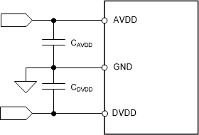
The device uses the analog supply voltage (AVDD) as the reference voltage for the analog to digital conversion. During the conversion process, the internal capacitors are switched to the AVDD pin as per the successive approximation algorithm. A voltage reference must be selected with low temperature drift, high output current drive and low output impedance. TI recommends a 3.3-µF (CAVDD), low equivalent series resistance (ESR) ceramic capacitor between the AVDD and GND pins. This decoupling capacitor provides the instantaneous charge required by the internal circuit during the conversion process and maintains a stable dc voltage on the AVDD pin.
See the Power Supply Recommendations and Layout Example sections for component recommendations and layout guidelines.
 Figure 34. Reference for the Device
8.3.4 ADC Transfer Function
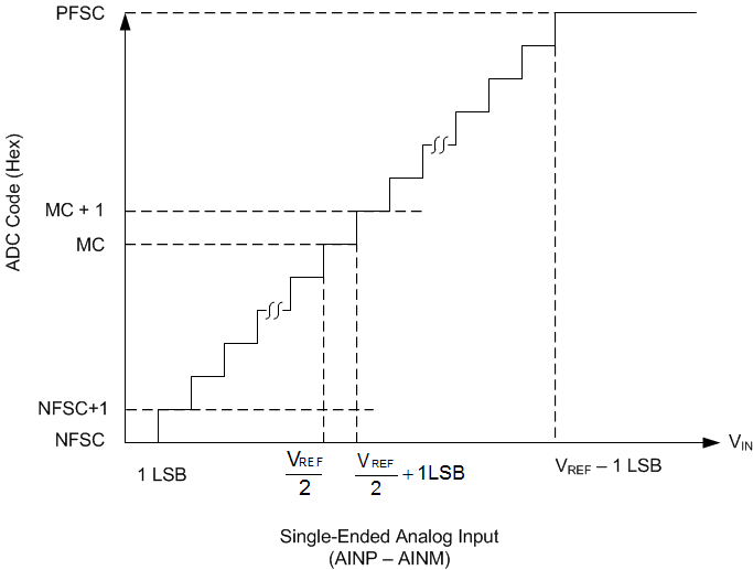
The device supports a unipolar, single-ended analog input signal. The output is in straight binary format. Figure 35 and Table 2 show the ideal transfer characteristics for the device.
The least significant bit for the device is given by:
where
- VREF = Voltage applied between the AVDD and GND pins
- N = 12
 Figure 35. Ideal Transfer Characteristics
Table 2. Transfer Characteristics
| INPUT VOLTAGE (AINP – AINM) | CODE | DESCRIPTION | IDEAL OUTPUT CODE (Hex) |
|---|---|---|---|
| ≤ 1 LSB | NFSC | Negative full-scale code | 000 |
| 1 LSB to 2 LSB | NFSC + 1 | — | 001 |
| VREF / 2 to VREF / 2 + 1 LSB | MC | Mid code | 7FF |
| VREF / 2 + 1 LSB to VREF / 2 + 2 LSB | MC + 1 | — | 800 |
| ≥ VREF – 1 LSB | PFSC | Positive full-scale code | FFF |
8.4 Device Functional Modes
The device supports a simple, SPI-compatible interface to the external host. On power-up, the device is in the ACQ state. The CS signal defines one conversion and serial data transfer frame. A frame starts with a CS falling edge and ends with a CS rising edge. The SDO pin is tri-stated when CS is high. With CS low, the clock provided on the SCLK pin is used for conversion and data transfer. Output data are available on the SDO pin.
As shown in Figure 36, the device supports three functional states: acquisition (ACQ), conversion (CNV), and offset calibration (OFFCAL). The device status depends on the CS and SCLK signals provided by the host controller.
 Figure 36. Functional State Diagram
8.4.1 ACQ State
In the ACQ state, switches SW1 and SW2 connected to the analog input pins close and the device acquires the analog input signal on CS1 and CS2. The device enters ACQ state at power-up, at the end of every conversion, and after completing the offset calibration. A CS falling edge takes the device from the ACQ state to the CNV state.
The device consumes extremely low power from the AVDD and DVDD power supplies when in ACQ state.
8.4.2 CNV State
In the CNV state, the device uses the external clock to convert the sampled analog input signal to an equivalent digital code as per the transfer function illustrated in Figure 35. The conversion process requires a minimum of 15 SCLK falling edges to be provided within the frame. After the end of conversion process, the device automatically moves from the CNV state to the ACQ state. For acquisition of the next sample, a minimum time of tACQ must be provided.
Figure 37 shows a detailed timing diagram for the serial interface. In the first serial transfer frame after power-up, the device provides the first data as all zeros. In any frame, the clocks provided on the SCLK pin are also used to transfer the output data for the previous conversion. A leading 0 is output on the SDO pin on the CS falling edge. The most significant bit (MSB) of the output data is launched on the SDO pin on the rising edge after the first SCLK falling edge. Subsequent output bits are launched on the subsequent rising edges provided on SCLK. When all 12 output bits are shifted out, the device outputs 0's on the subsequent SCLK rising edges. The device enters the ACQ state after 15 clocks and a minimum time of tACQ must be provided for acquiring the next sample. If the device is provided with less than 15 SCLK falling edges in the present serial transfer frame, the device provides an invalid conversion result in the next serial transfer frame.
 Figure 37. Serial Interface Timing Diagram
8.4.3 OFFCAL State
In the offset calibration (OFFCAL) state, the sampling capacitors are disconnected from the analog input pins (AINP and AINM) and the device calibrates and corrects for any internal offset errors. The offset calibration is effective for all subsequent conversions until the device is powered off. An offset calibration cycle is recommended at power-up and whenever there is a significant change in the operating conditions for the device (such as in the AVDD voltage and operating temperature).
The host controller must provide a serial transfer frame as described in Figure 38 or in Figure 39 to enter the OFFCAL state.
8.4.3.1 Offset Calibration on Power-Up
On power-up, the host must provide 24 SCLKs in the first serial transfer to enter the OFFCAL state. The device provides 0's on SDO during offset calibration. For acquisition of the next sample, a minimum time of tACQ must be provided.
If the host controller starts the offset calibration process but then pulls the CS pin high before providing 24 SCLKs, then the offset calibration process is aborted and the device enters the ACQ state. Figure 38 and Table 3 provide the timing for offset calibration on power-up.
 Figure 38. Timing for Offset Calibration on Power-Up
Table 3. Timing Specifications for Offset Calibration on Power-Up(1)
| MIN | TYP | MAX | UNIT | ||
|---|---|---|---|---|---|
| tcycle | Cycle time for offset calibration on power-up | 24 × tCLK + tACQ | ns | ||
| tACQ | Acquisition time | 80 | ns | ||
| fSCLK | Frequency of SCLK | 60 | MHz | ||
8.4.3.2 Offset Calibration During Normal Operation
During normal operation, the host must provide 64 SCLKs in the serial transfer frame to enter the OFFCAL state. The device provides the conversion result for the previous sample during the first 15 SCLKs and 0's on SDO for the rest of the SCLKs in the serial transfer frame. For acquisition of the next sample, a minimum time of tACQ must be provided.
If the host controller provides more than 15 SCLKs but pulls the CS high before providing 64 SCLKs, then the offset calibration process is aborted and the device enters the ACQ state. Figure 39 and Table 4 provide the timing for offset calibration during normal operation.
 Figure 39. Timing for Offset Calibration During Normal Operation
Table 4. Timing Specifications for Offset Calibration During Normal Operation(1)
| MIN | TYP | MAX | UNIT | ||
|---|---|---|---|---|---|
| tcycle | Cycle time for offset calibration on power-up | 64 × tCLK + tACQ | ns | ||
| tACQ | Acquisition time | 80 | ns | ||
| fSCLK | Frequency of SCLK | 60 | MHz | ||