SBAS819 December 2017 ADS7047
PRODUCTION DATA.
- 1 Features
- 2 Applications
- 3 Description
- 4 Revision History
- 5 Pin Configuration and Functions
- 6 Specifications
- 7 Parameter Measurement Information
- 8 Detailed Description
- 9 Application and Implementation
- 10Power Supply Recommendations
- 11Layout
- 12Device and Documentation Support
- 13Mechanical, Packaging, and Orderable Information
Package Options
Mechanical Data (Package|Pins)
- RUG|8
Thermal pad, mechanical data (Package|Pins)
- RUG|8
Orderable Information
1 Features
- 3-MSPS Throughput
- Small Package Size:
- X2QFN-8 Package (1.5 mm × 1.5 mm)
- Fully Differential Input Range: ±AVDD
- Wide Operating Range:
- AVDD: 2.35 V to 3.6 V
- DVDD: 1.65 V to 3.6 V (Independent of AVDD)
- Temperature Range: –40°C to +125°C
- Excellent Performance:
- 12-Bit NMC DNL, ±0.2-LSB INL
- 72.8-dB SINAD at 2 kHz
- 71.7-dB SINAD at 1 MHz
- Low Power Consumption:
- 4 mW at 3 MSPS With 3.3-V AVDD
- 130 µW at 100 kSPS With 3.3-V AVDD
- 74 µW at 100 kSPS With 2.5-V AVDD
- Integrated Offset Calibration
- SPI-Compatible Serial Interface: 60 MHz
- JESD8-7A Compliant Digital I/O
2 Applications
- Optical Encoders
- Sonar Receivers
- Fish Finders
- I-Q Demodulators
- Optical Line Cards and Modules
- Thermal Imaging Cameras
- Ultrasonic Flow Meters
- Handheld Radios
3 Description
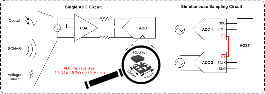
The ADS7047 device belongs to a family of pin-to-pin compatible, high-speed, low-power, single-channel successive-approximation register (SAR) type analog-to-digital converters (ADCs). The device family includes multiple resolutions, throughputs, and analog input variants (see Table 1 for a list of devices).
The ADS7047 is a 12-bit, 3-MSPS SAR ADC that supports fully-differential inputs in the range of ±AVDD, for AVDD in the range of 2.35 V to 3.6 V.
The internal offset calibration feature maintains excellent offset specifications over the entire AVDD and temperature operating range.
The device supports an SPI-compatible serial interface that is controlled by the CS and SCLK signals. The input signal is sampled with the CS falling edge and SCLK is used for both conversion and serial data output. The device supports a wide digital supply range (1.65 V to 3.6 V), enabling direct interfacing to a variety of host controllers. The ADS7047 complies with the JESD8-7A standard for a normal DVDD range (1.65 V to 1.95 V).
The ADS7047 is available in an 8-pin, small, X2QFN package and is specified over the extended industrial temperature range (–40°C to +125°C). The small form-factor and extremely-low power consumption make this device suitable for space-constrained and battery-powered applications that require high-speed, high-resolution data acquisition.
Device Information(1)
| PART NAME | PACKAGE | BODY SIZE (NOM) |
|---|---|---|
| ADS7047 | X2QFN (8) | 1.50 mm × 1.50 mm |
- For all available packages, see the orderable addendum at the end of the datasheet.
Typical Application
