SBAS928C February 2020 – September 2023 ADS7066
PRODUCTION DATA
- 1
- 1 Features
- 2 Applications
- 3 Description
- 4 Revision History
- 5 Pin Configuration and Functions
- 6 Specifications
-
7 Detailed Description
- 7.1 Overview
- 7.2 Functional Block Diagram
- 7.3 Feature Description
- 7.4 Device Functional Modes
- 7.5 ADS7066 Registers
- 8 Application and Implementation
- 9 Device and Documentation Support
- 10Mechanical, Packaging, and Orderable Information
Package Options
Mechanical Data (Package|Pins)
Thermal pad, mechanical data (Package|Pins)
- RTE|16
Orderable Information
5 Pin Configuration and Functions
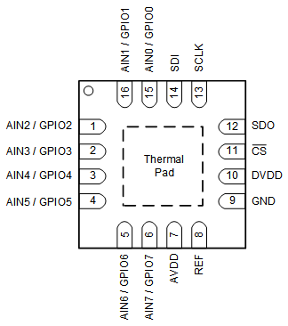
 Figure 5-1 RTE Package,16-Pin WQFN(Top View)
Table 5-1 Pin Functions: RTE Package
| PIN | TYPE(1) | DESCRIPTION | |
|---|---|---|---|
| NAME | RTE | ||
| AIN0/GPIO0 | 15 | AI, DI, DO | Channel 0; configurable as either an analog input (default) or general-purpose input/output (GPIO). |
| AIN1/GPIO1 | 16 | AI, DI, DO | Channel 1; configurable as either an analog input (default) or GPIO. |
| AIN2/GPIO2 | 1 | AI, DI, DO | Channel 2; configurable as either an analog input (default) or GPIO. |
| AIN3/GPIO3 | 2 | AI, DI, DO | Channel 3; configurable as either an analog input (default) or GPIO. |
| AIN4/GPIO4 | 3 | AI, DI, DO | Channel 4; configurable as either an analog input (default) or GPIO. |
| AIN5/GPIO5 | 4 | AI, DI, DO | Channel 5; configurable as either an analog input (default) or GPIO. |
| AIN6/GPIO6 | 5 | AI, DI, DO | Channel 6; configurable as either an analog input (default) or GPIO. |
| AIN7/GPIO7 | 6 | AI, DI, DO | Channel 7; configurable as either an analog input (default) or GPIO. |
| AVDD | 7 | P | Analog supply voltage. Connect a 1-µF capacitor to GND. |
| CS | 11 | DI | Chip-select input pin; active low. The device takes control of the data bus when CS is low. The SDO pin goes to Hi-Z when CS is high. |
| DVDD | 10 | P | Digital I/O supply voltage. Connect a 1-µF capacitor to GND. |
| GND | 9 | P | Ground for power supply, all analog and digital signals are referred to this pin. |
| REF | 8 | P | Internal reference buffer output; external reference input. Connect a 1-µF capacitor to GND. |
| SCLK | 13 | DI | Clock input pin for the SPI interface. |
| SDI | 14 | DI | Serial data input pin for SPI interface. |
| SDO | 12 | DO | Serial data output pin for SPI interface. |
| Thermal Pad | Pad | P | Exposed thermal pad. Connect to ground. |
(1) AI = analog input, DI = digital input, DO = digital output,
P = power supply.
 Figure 5-2 YBH Package,16-Pin DSBGA
(Top View)
Table 5-2 Pin Functions: YBH
Package
| PIN | TYPE(1) | DESCRIPTION | |
|---|---|---|---|
| YBH | NAME | ||
| A1 | AIN5/GPIO5 | AI, DI, DO | Channel 5; configurable as either an analog input (default) or GPIO. |
| A2 | DVDD | P | Digital I/O supply voltage. Connect a 1-µF capacitor to GND. |
| A3 | AVDD | P | Analog supply voltage. Connect a 1-µF capacitor to GND. |
| A4 | REF | P | Internal reference buffer output; external reference input. Connect a 1-µF capacitor to GND. |
| B1 | AIN4/GPIO4 | AI, DI, DO | Channel 4; configurable as either an analog input (default) or GPIO. |
| B2 | AIN6/GPIO6 | AI, DI, DO | Channel 6; configurable as either an analog input (default) or GPIO. |
| B3 | AIN7/GPIO7 | AI, DI, DO | Channel 7; configurable as either an analog input (default) or GPIO. |
| B4 | GND | P | Ground for power supply, all analog and digital signals are referred to this pin. |
| C1 | AIN3/GPIO3 | AI, DI, DO | Channel 3; configurable as either an analog input (default) or GPIO. |
| C2 | AIN1/GPIO1 | AI, DI, DO | Channel 1; configurable as either an analog input (default) or GPIO. |
| C3 | AIN0/GPIO0 | AI, DI, DO | Channel 0; configurable as either an analog input (default) or general-purpose input/output (GPIO). |
| C4 | CS | DI | Chip-select input pin; active low. The device takes control of the data bus when CS is low. The SDO pin goes to Hi-Z when CS is high. |
| D1 | AIN2/GPIO2 | AI, DI, DO | Channel 2; configurable as either an analog input (default) or GPIO. |
| D2 | SDI | DI | Serial data input pin for SPI interface. |
| D3 | SDO | DO | Serial data output pin for SPI interface. |
| D4 | SCLK | DI | Clock input pin for the SPI interface. |
(1) AI = analog input, DI = digital input, DO = digital output, P =
power supply.