SBASA78B March   2021  – September 2024 ADS7067

PRODUCTION DATA  

  1.   1
  2. Features
  3. Applications
  4. Description
  5. Pin Configuration and Functions
  6. Specifications
    1. 5.1 Absolute Maximum Ratings
    2. 5.2 ESD Ratings
    3. 5.3 Recommended Operating Conditions
    4. 5.4 Thermal Information
    5. 5.5 Electrical Characteristics
    6. 5.6 Timing Requirements
    7. 5.7 Switching Characteristics
    8. 5.8 Timing Diagrams
    9. 5.9 Typical Characteristics
  7. Detailed Description
    1. 6.1 Overview
    2. 6.2 Functional Block Diagram
    3. 6.3 Feature Description
      1. 6.3.1  Analog Input and Multiplexer
      2. 6.3.2  Reference
        1. 6.3.2.1 External Reference
        2. 6.3.2.2 Internal Reference
      3. 6.3.3  ADC Transfer Function
      4. 6.3.4  ADC Offset Calibration
      5. 6.3.5  Programmable Averaging Filters
      6. 6.3.6  CRC on Data Interface
      7. 6.3.7  Oscillator and Timing Control
      8. 6.3.8  Diagnostic Modes
        1. 6.3.8.1 Bit-Walk Test Mode
        2. 6.3.8.2 Fixed Voltage Test Mode
      9. 6.3.9  Output Data Format
        1. 6.3.9.1 Status Flags
        2. 6.3.9.2 Output CRC (Device to Host)
        3. 6.3.9.3 Input CRC (Host to Device)
      10. 6.3.10 Device Programming
        1. 6.3.10.1 Enhanced-SPI Interface
        2. 6.3.10.2 Daisy-Chain Mode
        3. 6.3.10.3 Register Read/Write Operation
          1. 6.3.10.3.1 Register Write
          2. 6.3.10.3.2 Register Read
            1. 6.3.10.3.2.1 Register Read With CRC
    4. 6.4 Device Functional Modes
      1. 6.4.1 Device Power-Up and Reset
      2. 6.4.2 Manual Mode
      3. 6.4.3 On-the-Fly Mode
      4. 6.4.4 Auto-Sequence Mode
    5. 6.5 ADS7067 Registers
  8. Application and Implementation
    1. 7.1 Application Information
    2. 7.2 Typical Application
      1. 7.2.1 Design Requirements
      2. 7.2.2 Detailed Design Procedure
        1. 7.2.2.1 Charge-Kickback Filter and ADC Amplifier
      3. 7.2.3 Application Curve
    3. 7.3 Power Supply Recommendations
      1. 7.3.1 AVDD and DVDD Supply Recommendations
    4. 7.4 Layout
      1. 7.4.1 Layout Guidelines
      2. 7.4.2 Layout Example
  9. Device and Documentation Support
    1. 8.1 Device Support
      1. 8.1.1 Development Support
    2. 8.2 Documentation Support
      1. 8.2.1 Related Documentation
    3. 8.3 Receiving Notification of Documentation Updates
    4. 8.4 Support Resources
    5. 8.5 Trademarks
    6. 8.6 Electrostatic Discharge Caution
    7. 8.7 Glossary
  10. Revision History
  11. 10Mechanical, Packaging, and Orderable Information

Package Options

Mechanical Data (Package|Pins)
Thermal pad, mechanical data (Package|Pins)
Orderable Information

Typical Characteristics

at TA = 25°C, AVDD = 5 V, DVDD = 1.65 V to 5.5 V, and maximum throughput (unless otherwise noted)
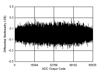
ADS7067 Typical
            DNL
Typical DNL = ±0.4 LSB
Figure 5-3 Typical DNL
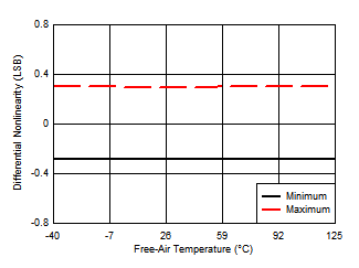
ADS7067 DNL vs
            Temperature
 
Figure 5-5 DNL vs Temperature
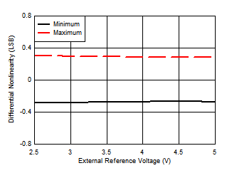
ADS7067 DNL vs External
            Reference Voltage
 
Figure 5-7 DNL vs External Reference Voltage
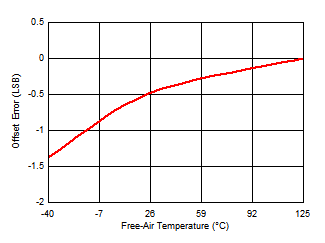
ADS7067 Offset Error vs
            Temperature
 
Figure 5-9 Offset Error vs Temperature
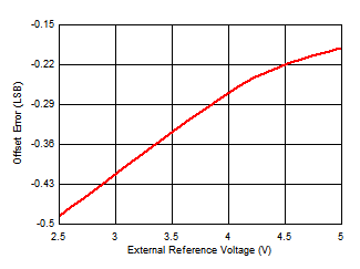
ADS7067 Offset Error vs
            External Reference Voltage
 
Figure 5-11 Offset Error vs External Reference Voltage
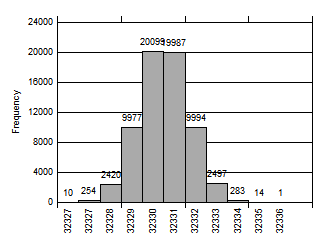
ADS7067 DC Input
            Histogram
Standard deviation = 1.05 LSB
Figure 5-13 DC Input Histogram
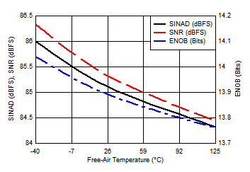
ADS7067 Noise
            Performance vs Temperature
 
Figure 5-15 Noise Performance vs Temperature
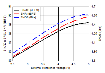
ADS7067 Noise
            Performance vs External Reference Voltage
 
Figure 5-17 Noise Performance vs External Reference Voltage
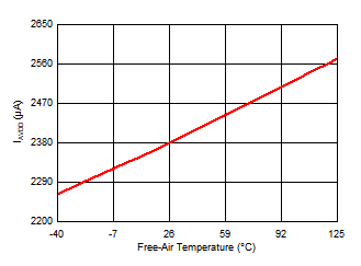
ADS7067 Analog Supply
            Current vs Temperature
AVDD = 5 V
Figure 5-19 Analog Supply Current vs Temperature
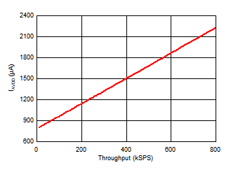
ADS7067 Analog Supply
            Current vs Throughput
 
Figure 5-21 Analog Supply Current vs Throughput
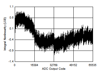
ADS7067 Typical
            INL
Typical INL = ±1 LSB
Figure 5-4 Typical INL
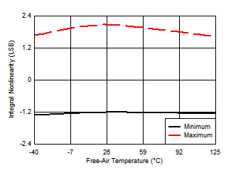
ADS7067 INL vs
            Temperature
 
Figure 5-6 INL vs Temperature
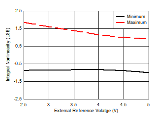
ADS7067 INL vs External
            Reference Voltage
 
Figure 5-8 INL vs External Reference Voltage
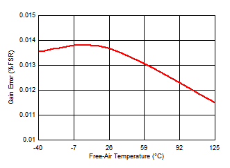
ADS7067 Gain Error vs
            Temperature
 
Figure 5-10 Gain Error vs Temperature
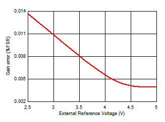
ADS7067 Gain Error vs
            External Reference Voltage
 
Figure 5-12 Gain Error vs External Reference Voltage
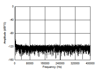
ADS7067 Typical
            FFT
fIN = 2 kHz, SNR = 85.3 dBFS, THD = –97 dB
Figure 5-14 Typical FFT
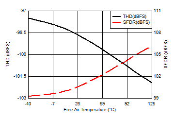
ADS7067 Distortion
            Performance vs Temperature
 
Figure 5-16 Distortion Performance vs Temperature
ADS7067 Distortion
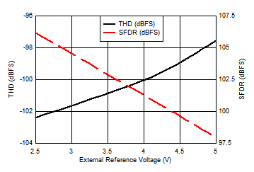
            Performance vs External Reference Voltage
 
Figure 5-18 Distortion Performance vs External Reference Voltage
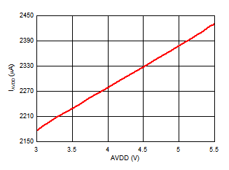
ADS7067 Analog Supply
            Current vs AVDD
TA = 25 °C
Figure 5-20 Analog Supply Current vs AVDD
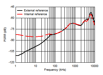
ADS7067 PSRR vs Frequency
 
Figure 5-22 PSRR vs Frequency