SBASA78B March   2021  – September 2024 ADS7067

PRODUCTION DATA  

  1.   1
  2. Features
  3. Applications
  4. Description
  5. Pin Configuration and Functions
  6. Specifications
    1. 5.1 Absolute Maximum Ratings
    2. 5.2 ESD Ratings
    3. 5.3 Recommended Operating Conditions
    4. 5.4 Thermal Information
    5. 5.5 Electrical Characteristics
    6. 5.6 Timing Requirements
    7. 5.7 Switching Characteristics
    8. 5.8 Timing Diagrams
    9. 5.9 Typical Characteristics
  7. Detailed Description
    1. 6.1 Overview
    2. 6.2 Functional Block Diagram
    3. 6.3 Feature Description
      1. 6.3.1  Analog Input and Multiplexer
      2. 6.3.2  Reference
        1. 6.3.2.1 External Reference
        2. 6.3.2.2 Internal Reference
      3. 6.3.3  ADC Transfer Function
      4. 6.3.4  ADC Offset Calibration
      5. 6.3.5  Programmable Averaging Filters
      6. 6.3.6  CRC on Data Interface
      7. 6.3.7  Oscillator and Timing Control
      8. 6.3.8  Diagnostic Modes
        1. 6.3.8.1 Bit-Walk Test Mode
        2. 6.3.8.2 Fixed Voltage Test Mode
      9. 6.3.9  Output Data Format
        1. 6.3.9.1 Status Flags
        2. 6.3.9.2 Output CRC (Device to Host)
        3. 6.3.9.3 Input CRC (Host to Device)
      10. 6.3.10 Device Programming
        1. 6.3.10.1 Enhanced-SPI Interface
        2. 6.3.10.2 Daisy-Chain Mode
        3. 6.3.10.3 Register Read/Write Operation
          1. 6.3.10.3.1 Register Write
          2. 6.3.10.3.2 Register Read
            1. 6.3.10.3.2.1 Register Read With CRC
    4. 6.4 Device Functional Modes
      1. 6.4.1 Device Power-Up and Reset
      2. 6.4.2 Manual Mode
      3. 6.4.3 On-the-Fly Mode
      4. 6.4.4 Auto-Sequence Mode
    5. 6.5 ADS7067 Registers
  8. Application and Implementation
    1. 7.1 Application Information
    2. 7.2 Typical Application
      1. 7.2.1 Design Requirements
      2. 7.2.2 Detailed Design Procedure
        1. 7.2.2.1 Charge-Kickback Filter and ADC Amplifier
      3. 7.2.3 Application Curve
    3. 7.3 Power Supply Recommendations
      1. 7.3.1 AVDD and DVDD Supply Recommendations
    4. 7.4 Layout
      1. 7.4.1 Layout Guidelines
      2. 7.4.2 Layout Example
  9. Device and Documentation Support
    1. 8.1 Device Support
      1. 8.1.1 Development Support
    2. 8.2 Documentation Support
      1. 8.2.1 Related Documentation
    3. 8.3 Receiving Notification of Documentation Updates
    4. 8.4 Support Resources
    5. 8.5 Trademarks
    6. 8.6 Electrostatic Discharge Caution
    7. 8.7 Glossary
  10. Revision History
  11. 10Mechanical, Packaging, and Orderable Information

Package Options

Mechanical Data (Package|Pins)
Thermal pad, mechanical data (Package|Pins)
Orderable Information

On-the-Fly Mode

In the on-the-fly mode of operation, as shown in Figure 6-14, the analog input channel is selected using the first five bits on SDI without waiting for the CS rising edge. Thus, the ADC samples the newly selected channel on the CS rising edge and there is no latency between the channel selection and the ADC output data. Table 6-8 lists the channel selection commands for this mode.
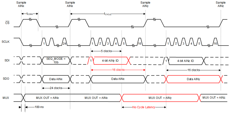
ADS7067 Starting a Conversion and Reading data in On-the-Fly ModeFigure 6-14 Starting a Conversion and Reading data in On-the-Fly Mode
Table 6-8 On-the-Fly Mode Channel Selection Commands
SDI BITS[15:11]SDI BITS [10:0]DESCRIPTION
1 0000Don't careSelect analog input 0
1 0001Don't careSelect analog input 1
1 0010Don't careSelect analog input 2
1 0011Don't careSelect analog input 3
1 0100Don't careSelect analog input 4
1 0101Don't careSelect analog input 5
1 0110Don't careSelect analog input 6
1 0111Don't careSelect analog input 7
1 1000 to 1 1111Don't careReserved

The number of clocks required for reading the output data depends on the device output data frame size; see the Output Data Format section for more details.