SBASA78B March   2021  – September 2024 ADS7067

PRODUCTION DATA  

  1.   1
  2. Features
  3. Applications
  4. Description
  5. Pin Configuration and Functions
  6. Specifications
    1. 5.1 Absolute Maximum Ratings
    2. 5.2 ESD Ratings
    3. 5.3 Recommended Operating Conditions
    4. 5.4 Thermal Information
    5. 5.5 Electrical Characteristics
    6. 5.6 Timing Requirements
    7. 5.7 Switching Characteristics
    8. 5.8 Timing Diagrams
    9. 5.9 Typical Characteristics
  7. Detailed Description
    1. 6.1 Overview
    2. 6.2 Functional Block Diagram
    3. 6.3 Feature Description
      1. 6.3.1  Analog Input and Multiplexer
      2. 6.3.2  Reference
        1. 6.3.2.1 External Reference
        2. 6.3.2.2 Internal Reference
      3. 6.3.3  ADC Transfer Function
      4. 6.3.4  ADC Offset Calibration
      5. 6.3.5  Programmable Averaging Filters
      6. 6.3.6  CRC on Data Interface
      7. 6.3.7  Oscillator and Timing Control
      8. 6.3.8  Diagnostic Modes
        1. 6.3.8.1 Bit-Walk Test Mode
        2. 6.3.8.2 Fixed Voltage Test Mode
      9. 6.3.9  Output Data Format
        1. 6.3.9.1 Status Flags
        2. 6.3.9.2 Output CRC (Device to Host)
        3. 6.3.9.3 Input CRC (Host to Device)
      10. 6.3.10 Device Programming
        1. 6.3.10.1 Enhanced-SPI Interface
        2. 6.3.10.2 Daisy-Chain Mode
        3. 6.3.10.3 Register Read/Write Operation
          1. 6.3.10.3.1 Register Write
          2. 6.3.10.3.2 Register Read
            1. 6.3.10.3.2.1 Register Read With CRC
    4. 6.4 Device Functional Modes
      1. 6.4.1 Device Power-Up and Reset
      2. 6.4.2 Manual Mode
      3. 6.4.3 On-the-Fly Mode
      4. 6.4.4 Auto-Sequence Mode
    5. 6.5 ADS7067 Registers
  8. Application and Implementation
    1. 7.1 Application Information
    2. 7.2 Typical Application
      1. 7.2.1 Design Requirements
      2. 7.2.2 Detailed Design Procedure
        1. 7.2.2.1 Charge-Kickback Filter and ADC Amplifier
      3. 7.2.3 Application Curve
    3. 7.3 Power Supply Recommendations
      1. 7.3.1 AVDD and DVDD Supply Recommendations
    4. 7.4 Layout
      1. 7.4.1 Layout Guidelines
      2. 7.4.2 Layout Example
  9. Device and Documentation Support
    1. 8.1 Device Support
      1. 8.1.1 Development Support
    2. 8.2 Documentation Support
      1. 8.2.1 Related Documentation
    3. 8.3 Receiving Notification of Documentation Updates
    4. 8.4 Support Resources
    5. 8.5 Trademarks
    6. 8.6 Electrostatic Discharge Caution
    7. 8.7 Glossary
  10. Revision History
  11. 10Mechanical, Packaging, and Orderable Information

Package Options

Mechanical Data (Package|Pins)
Thermal pad, mechanical data (Package|Pins)
Orderable Information

Programmable Averaging Filters

The ADS7067 features a programmable averaging filter that can be used to average analog input samples to output a higher resolution measurement. The averaging filter can be enabled by programming the OSR[2:0] bits in the OSR_CFG register to the averaging factor desired. The averaging configuration is common to all analog input channels. As shown in Figure 6-3, the output of the averaging filter is 20 bits long. In manual mode and auto-sequence mode of conversion, only the first conversion for the selected analog input channel must be initiated by the host, as shown in Figure 6-3; any remaining conversions are generated internally. The time (tAVG) required to complete the averaging operation is determined by the sampling speed and number of samples to be averaged; see the Oscillator and Timing Control section for more details. After completion, the averaged 20-bit result, as shown in Figure 6-3, can be read-out. For information on the programmable averaging filters and performance results see the Resolution-Boosting ADS7066 Using Programmable Averaging Filter application report.

In autonomous mode of operation, samples from analog input channels that are enabled in the AUTO_SEQ_CH_SEL register are averaged sequentially.
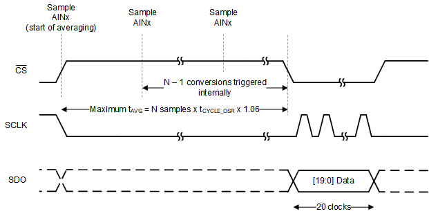
ADS7067 Averaged Output DataFigure 6-3 Averaged Output Data