SBAS456B December 2008 – January 2016 ADS7828-Q1
PRODUCTION DATA.
- 1 Features
- 2 Applications
- 3 Description
- 4 Revision History
- 5 Pin Configuration and Functions
-
6 Specifications
- 6.1 Absolute Maximum Ratings
- 6.2 ESD Ratings
- 6.3 Recommended Operating Conditions
- 6.4 Thermal Information
- 6.5 Electrical Characteristics for ADS7828E
- 6.6 Electrical Characteristics for ADS7828EB
- 6.7 Electrical Characteristics for ADS7828E
- 6.8 Electrical Characteristics for ADS7828EB
- 6.9 Switching Characteristics
- 6.10 Typical Characteristics
- 7 Detailed Description
- 8 Application and Implementation
- 9 Power Supply Recommendations
- 10Layout
- 11Device and Documentation Support
- 12Mechanical, Packaging, and Orderable Information
Package Options
Mechanical Data (Package|Pins)
- PW|16
Thermal pad, mechanical data (Package|Pins)
Orderable Information
6 Specifications
6.1 Absolute Maximum Ratings
over operating free-air temperature range, unless otherwise noted.(1)(2)| MIN | MAX | UNIT | |||
|---|---|---|---|---|---|
| VDD | Supply voltage | –0.3 | 6 | V | |
| VIN | Digital input voltage | –0.3 | 0.3 | V | |
| θJA | Thermal impedance, junction to free air(3)(4) | 108.4 | °C/W | ||
| TA | Operating free-air temperature | –40 | 85 | °C | |
| Tlead | Lead temperature during soldering | Vapor phase (60 seconds) | 215 | °C | |
| Infrared (15 seconds) | 220 | °C | |||
| TJ | Operating virtual-junction temperature | 150 | °C | ||
| Tstg | Storage temperature | –65 | 150 | °C | |
(1) Stresses beyond those listed under Absolute Maximum Ratings may cause permanent damage to the device. These are stress ratings only, which do not imply functional operation of the device at these or any other conditions beyond those indicated under Recommended Operating Conditions. Exposure to absolute-maximum-rated conditions for extended periods may affect device reliability.
(2) All voltages are with respect to the GND terminal.
(3) The package thermal impedance is calculated in accordance with JESD 51-7.
(4) Maximum power dissipation is a function of TJ(max), θJA, and TA. The maximum allowable power dissipation at any allowable ambient temperature is PD = (TJ(max) – TA)/θJA. Operating at the absolute maximum TJ of 150°C can impact reliability.
6.2 ESD Ratings
| VALUE | UNIT | |||
|---|---|---|---|---|
| V(ESD) | Electrostatic discharge | Human-body model (HBM), per AEC Q100-002(1) | ±2000 | V |
| Charged-device model (CDM), per AEC Q100-011 | ±1000 | |||
(1) AEC Q100-002 indicates that HBM stressing shall be in accordance with the ANSI/ESDA/JEDEC JS-001 specification.
6.3 Recommended Operating Conditions
over operating free-air temperature range (unless otherwise noted)| MIN | NOM | MAX | UNIT | |||
|---|---|---|---|---|---|---|
| VDD | Supply Voltage | 2.7-V nominal | 2.7 | 3.6 | V | |
| 5-V nominal | 4.75 | 5 | 5.25 | |||
| VIN | Analog Input Voltage | Positive Input | –0.2 | +VDD + 0.2 | V | |
| Negative Input | –0.2 | 0.2 | ||||
| Full-scale differential (Positive input – Negative input) | 0 | VREF | ||||
| VIN(REF) | Voltage Reference Input voltage | 0.05 | +VDD | V | ||
| VIH | High-level digital input voltage | 0.7 × +VDD | +VDD + 0.5 | V | ||
| VIL | Low-level digital input voltage | –0.3 | 0.3 × +VDD | V | ||
| TA | Operating free-air temperature | –40 | 85 | °C | ||
6.4 Thermal Information
over operating free-air temperature range (unless otherwise noted)| THERMAL METRIC(1) | ADS7828-Q1 | UNIT | |
|---|---|---|---|
| PW (TSSOP) | |||
| 16 PINS | |||
| RθJA | Junction-to-ambient thermal resistance | 102.1 | °C/W |
| RθJC(top) | Junction-to-case (top) thermal resistance | 37.2 | °C/W |
| RθJB | Junction-to-board thermal resistance | 47.1 | °C/W |
| ψJT | Junction-to-top characterization parameter | 2.9 | °C/W |
| ψJB | Junction-to-board characterization parameter | 46.5 | °C/W |
(1) For more information about traditional and new thermal metrics, see the Semiconductor and IC Package Thermal Metrics application report, SPRA953.
6.5 Electrical Characteristics for ADS7828E
+VDD = 2.7 V, VREF = 2.5 V, SCL clock frequency = 3.4 MHz (high-speed mode), over operating free-air temperature range, unless otherwise noted.| PARAMETER | TEST CONDITIONS | MIN | TYP | MAX | UNIT | |
|---|---|---|---|---|---|---|
| Analog Input | ||||||
| Ileak | Leakage current | ±1 | µA | |||
| CI | 25 | pF | ||||
| Overall Performance | ||||||
| No missing codes | 12 | bits | ||||
| Integral linearity error | ±1 | ±2 | LSB(1) | |||
| Differential linearity error | ±1 | LSB | ||||
| Offset error | ±1 | ±3 | LSB | |||
| Offset error match | ±0.2 | ±1 | LSB | |||
| Gain error | ±1 | ±4 | LSB | |||
| Gain error match | ±0.2 | ±1 | LSB | |||
| Vn | Noise | RMS | 33 | µV | ||
| PSRR | Power-supply ripple rejection | 82 | dB | |||
| Sampling Dynamics | ||||||
| Throughput frequency | High-speed mode: SCL = 3.4 MHz | 50 | kHz | |||
| Fast mode: SCL = 400 kHz | 8 | |||||
| Standard mode: SCL = 100 kHz | 2 | |||||
| Conversion time | 6 | µs | ||||
| AC Accuracy | ||||||
| THD | Total harmonic distortion(2) | VIN = 25 VPP at 10 kHz | –82 | dB | ||
| Signal-to-noise ratio | VIN = 25 VPP at 10 kHz | 72 | dB | |||
| Signal-to-(noise + distortion) ratio | VIN = 25 VPP at 10 kHz | 71 | dB | |||
| Spurious-free dynamic range | VIN = 25 VPP at 10 kHz | 86 | dB | |||
| Channel-to-channel isolation | 120 | dB | ||||
| Voltage Reference Output | ||||||
| VO | Output voltage | 2.475 | 2.5 | 2.525 | V | |
| Internal reference drift | 15 | ppm/°C | ||||
| zo | Output impedance | Internal reference on | 110 | Ω | ||
| Internal reference off | 1 | GΩ | ||||
| IQ | Quiescent current | 850 | µA | |||
| Voltage Reference Input | ||||||
| rI | Input resistance | 1 | GΩ | |||
| Current drain | 20 | µA | ||||
| Digital Input and Output | ||||||
| VOL | Low-level output voltage | Minimum 3-mA sink current | 0.4 | V | ||
| IIH | High-level input current | VIH = +VDD + 0.5 V | 10 | µA | ||
| IIL | Low-level input current | VIL = –0.3 V | –10 | µA | ||
| Power Supply | ||||||
| IQ | Quiescent current | High-speed mode: SCL = 3.4 MHz | 225 | 320 | µA | |
| Fast mode: SCL = 400 kHz | 100 | |||||
| Standard mode: SCL = 100 kHz | 60 | |||||
| PO | Power dissipation | High-speed mode: SCL = 3.4 MHz | 675 | 1000 | µW | |
| Fast mode: SCL = 400 kHz | 300 | |||||
| Standard mode: SCL = 100 kHz | 180 | |||||
| Power-down current with wrong address selected | High-speed mode: SCL = 3.4 MHz | 70 | µA | |||
| Fast mode: SCL = 400 kHz | 25 | |||||
| Standard mode: SCL = 100 kHz | 6 | |||||
| IPD | Full power-down current | SCL pulled high, SDA pulled high | 400 | 3000 | nA | |
(1) LSB means Least Significant Bit; with VREF equal to 2.5 V, one LSB is 610 µV.
(2) THD is measured to the ninth harmonic.
6.6 Electrical Characteristics for ADS7828EB
+VDD = 2.7 V, VREF = 2.5 V, SCL clock frequency = 3.4 MHz (high-speed mode), over operating free-air temperature range, unless otherwise noted.| PARAMETER | TEST CONDITIONS | MIN | TYP | MAX | UNIT | |
|---|---|---|---|---|---|---|
| Analog Input | ||||||
| Ileak | Leakage current | ±1 | µA | |||
| CI | 25 | pF | ||||
| Overall Performance | ||||||
| No missing codes | 12 | bits | ||||
| Integral linearity error | ±0.5 | ±1 | LSB(1) | |||
| Differential linearity error | ±0.5 | –1 to 2 | LSB | |||
| Offset error | ±0.75 | ±2 | LSB | |||
| Offset error match | ±0.2 | ±1 | LSB | |||
| Gain error | ±0.75 | ±3 | LSB | |||
| Gain error match | ±0.2 | ±1 | LSB | |||
| Vn | Noise | RMS | 33 | µV | ||
| PSRR | Power-supply ripple rejection | 82 | dB | |||
| Sampling Dynamics | ||||||
| Throughput frequency | High-speed mode: SCL = 3.4 MHz | 50 | kHz | |||
| Fast mode: SCL = 400 kHz | 8 | |||||
| Standard mode: SCL = 100 kHz | 2 | |||||
| Conversion time | 6 | µs | ||||
| AC Accuracy | ||||||
| THD | Total harmonic distortion(2) | VIN = 25 VPP at 10 kHz | –82 | dB | ||
| Signal-to-noise ratio | VIN = 25 VPP at 10 kHz | 72 | dB | |||
| Signal-to-(noise + distortion) ratio | VIN = 25 VPP at 10 kHz | 71 | dB | |||
| Spurious-free dynamic range | VIN = 25 VPP at 10 kHz | 86 | dB | |||
| Channel-to-channel isolation | 120 | dB | ||||
| Voltage Reference Output | ||||||
| VO | Output voltage | 2.475 | 2.5 | 2.525 | V | |
| Internal reference drift | 15 | ppm/°C | ||||
| zo | Output impedance | Internal reference on | 110 | Ω | ||
| Internal reference off | 1 | GΩ | ||||
| IQ | Quiescent current | 850 | µA | |||
| Voltage Reference Input | ||||||
| rI | Input resistance | 1 | GΩ | |||
| Current drain | 20 | µA | ||||
| Digital Input and Output | ||||||
| VOL | Low-level output voltage | Minimum 3-mA sink current | 0.4 | V | ||
| IIH | High-level input current | VIH = +VDD + 0.5 V | 10 | µA | ||
| IIL | Low-level input current | VIL = –0.3 V | –10 | µA | ||
| Power Supply | ||||||
| IQ | Quiescent current | High-speed mode: SCL = 3.4 MHz | 225 | 320 | µA | |
| Fast mode: SCL = 400 kHz | 100 | |||||
| Standard mode: SCL = 100 kHz | 60 | |||||
| PO | Power dissipation | High-speed mode: SCL = 3.4 MHz | 675 | 1000 | µW | |
| Fast mode: SCL = 400 kHz | 300 | |||||
| Standard mode: SCL = 100 kHz | 180 | |||||
| Power-down current with wrong address selected | High-speed mode: SCL = 3.4 MHz | 70 | µA | |||
| Fast mode: SCL = 400 kHz | 25 | |||||
| Standard mode: SCL = 100 kHz | 6 | |||||
| IPD | Full power-down current | SCL pulled high, SDA pulled high | 400 | 3000 | nA | |
(1) LSB means Least Significant Bit; with VREF equal to 2.5 V, one LSB is 610 µV.
(2) THD is measured to the ninth harmonic.
6.7 Electrical Characteristics for ADS7828E
+VDD = 5 V, VREF = External 5 V, SCL clock frequency = 3.4 MHz (high-speed mode), over operating free-air temperature range, unless otherwise noted.| PARAMETER | TEST CONDITIONS | MIN | TYP | MAX | UNIT | |
|---|---|---|---|---|---|---|
| Analog Input | ||||||
| Ileak | Leakage current | ±1 | µA | |||
| CI | 25 | pF | ||||
| Overall Performance | ||||||
| No missing codes | 12 | bits | ||||
| Integral linearity error | ±1 | ±2 | LSB(1) | |||
| Differential linearity error | ±1 | LSB | ||||
| Offset error | ±1 | ±3 | LSB | |||
| Offset error match | ±1.5 | LSB | ||||
| Gain error | ±1 | ±3 | LSB | |||
| Gain error match | ±1 | LSB | ||||
| Vn | Noise | RMS | 33 | µV | ||
| PSRR | Power-supply ripple rejection | 82 | dB | |||
| Sampling Dynamics | ||||||
| Throughput frequency | High-speed mode: SCL = 3.4 MHz | 50 | kHz | |||
| Fast mode: SCL = 400 kHz | 8 | |||||
| Standard mode: SCL = 100 kHz | 2 | |||||
| Conversion time | 6 | µs | ||||
| AC Accuracy | ||||||
| THD | Total harmonic distortion(2) | VIN = 25 VPP at 10 kHz | –82 | dB | ||
| Signal-to-noise ratio | VIN = 25 VPP at 10 kHz | 72 | dB | |||
| Signal-to-(noise + distortion) ratio | VIN = 25 VPP at 10 kHz | 71 | dB | |||
| Spurious-free dynamic range | VIN = 25 VPP at 10 kHz | 86 | dB | |||
| Channel-to-channel isolation | 120 | dB | ||||
| Voltage Reference Output | ||||||
| VO | Output voltage | 2.475 | 2.5 | 2.525 | V | |
| Internal reference drift | 15 | ppm/°C | ||||
| zo | Output impedance | Internal reference on | 110 | Ω | ||
| Internal reference off | 1 | GΩ | ||||
| IQ | Quiescent current | 1300 | µA | |||
| Voltage Reference Input | ||||||
| rI | Input resistance | 1 | GΩ | |||
| Current drain | 20 | µA | ||||
| Digital Input and Output | ||||||
| VOL | Low-level output voltage | Minimum 3-mA sink current | 0.4 | V | ||
| IIH | High-level input current | VIH = +VDD + 0.5 V | 10 | µA | ||
| IIL | Low-level input current | VIL = –0.3 V | –10 | µA | ||
| Power Supply | ||||||
| IQ | Quiescent current | High-speed mode: SCL = 3.4 MHz | 750 | 100 | µA | |
| Fast mode: SCL = 400 kHz | 300 | |||||
| Standard mode: SCL = 100 kHz | 150 | |||||
| PO | Power dissipation | High-speed mode: SCL = 3.4 MHz | 3.75 | 5 | µW | |
| Fast mode: SCL = 400 kHz | 1.5 | |||||
| Standard mode: SCL = 100 kHz | 0.75 | |||||
| Power-down current with wrong address selected | High-speed mode: SCL = 3.4 MHz | 400 | µA | |||
| Fast mode: SCL = 400 kHz | 150 | |||||
| Standard mode: SCL = 100 kHz | 35 | |||||
| IPD | Full power-down current | SCL pulled high, SDA pulled high | 400 | 3000 | nA | |
(1) LSB means Least Significant Bit; with VREF equal to 5 V, one LSB is 1.22 mV.
(2) THD is measured to the ninth harmonic.
6.8 Electrical Characteristics for ADS7828EB
+VDD = 5 V, VREF = External 5 V, SCL clock frequency = 3.4 MHz (high-speed mode), over operating free-air temperature range, unless otherwise noted.| PARAMETER | TEST CONDITIONS | MIN | TYP | MAX | UNIT | |
|---|---|---|---|---|---|---|
| Analog Input | ||||||
| Ileak | Leakage current | ±1 | µA | |||
| CI | 25 | pF | ||||
| Overall Performance | ||||||
| No missing codes | 12 | bits | ||||
| Integral linearity error | ±0.5 | ±1 | LSB(1) | |||
| Differential linearity error | ±0.5 | –1 to 2 | LSB | |||
| Offset error | ±0.75 | ±2 | LSB | |||
| Offset error match | ±1 | LSB | ||||
| Gain error | ±0.75 | ±2 | LSB | |||
| Gain error match | ±1 | LSB | ||||
| Vn | Noise | RMS | 33 | µV | ||
| PSRR | Power-supply ripple rejection | 82 | dB | |||
| Sampling Dynamics | ||||||
| Throughput frequency | High-speed mode: SCL = 3.4 MHz | 50 | kHz | |||
| Fast mode: SCL = 400 kHz | 8 | |||||
| Standard mode: SCL = 100 kHz | 2 | |||||
| Conversion time | 6 | µs | ||||
| AC Accuracy | ||||||
| THD | Total harmonic distortion(2) | VIN = 25 VPP at 10 kHz | –82 | dB | ||
| Signal-to-noise ratio | VIN = 25 VPP at 10 kHz | 72 | dB | |||
| Signal-to-(noise + distortion) ratio | VIN = 25 VPP at 10 kHz | 71 | dB | |||
| Spurious-free dynamic range | VIN = 25 VPP at 10 kHz | 86 | dB | |||
| Channel-to-channel isolation | 120 | dB | ||||
| Voltage Reference Output | ||||||
| VO | Output voltage | 2.475 | 2.5 | 2.525 | V | |
| Internal reference drift | 15 | ppm/°C | ||||
| zo | Output impedance | Internal reference on | 110 | Ω | ||
| Internal reference off | 1 | GΩ | ||||
| IQ | Quiescent current | 1300 | µA | |||
| Voltage Reference Input | ||||||
| rI | Input resistance | 1 | GΩ | |||
| Current drain | 20 | µA | ||||
| Digital Input and Output | ||||||
| VOL | Low-level output voltage | Minimum 3-mA sink current | 0.4 | V | ||
| IIH | High-level input current | VIH = +VDD + 0.5 V | 10 | µA | ||
| IIL | Low-level input current | VIL = –0.3 V | –10 | µA | ||
| Power Supply | ||||||
| IQ | Quiescent current | High-speed mode: SCL = 3.4 MHz | 750 | 1000 | µA | |
| Fast mode: SCL = 400 kHz | 300 | |||||
| Standard mode: SCL = 100 kHz | 150 | |||||
| PO | Power dissipation | High-speed mode: SCL = 3.4 MHz | 3.75 | 5 | µW | |
| Fast mode: SCL = 400 kHz | 1.5 | |||||
| Standard mode: SCL = 100 kHz | 0.75 | |||||
| Power-down current with wrong address selected | High-speed mode: SCL = 3.4 MHz | 400 | µA | |||
| Fast mode: SCL = 400 kHz | 150 | |||||
| Standard mode: SCL = 100 kHz | 35 | |||||
| IPD | Full power-down current | SCL pulled high, SDA pulled high | 400 | 3000 | nA | |
(1) LSB means Least Significant Bit; with VREF equal to 5 V, one LSB is 1.22 mV.
(2) THD is measured to the ninth harmonic.
6.9 Switching Characteristics
+VDD = 2.7 V, over operating free-air temperature range, unless otherwise noted.(1)(2) See Figure 1.| PARAMETER | TEST CONDITIONS | MIN | MAX | UNIT | ||
|---|---|---|---|---|---|---|
| fSCL | SCL clock frequency | Standard mode | 100 | kHz | ||
| Fast mode | 400 | |||||
| High-speed mode | Cb = 100 pF max | 3.4 | MHz | |||
| Cb = 400 pF max | 1.7 | |||||
| tBUF | Bus free time between Stop and Start conditions | Standard mode | 4.7 | μs | ||
| Fast mode | 1.3 | |||||
| tHD; STA | Hold time (repeated) Start condition | Standard mode | 4 | μs | ||
| Fast mode | 600 | ns | ||||
| High-speed mode | 160 | |||||
| tlow | Low period of the SCL clock | Standard mode | 4.7 | μs | ||
| Fast mode | 1.3 | |||||
| High-speed mode(3) | Cb = 100 pF max | 160 | ns | |||
| Cb = 400 pF max | 320 | |||||
| thigh | High period of the SCL clock | Standard mode | 4 | μs | ||
| Fast mode | 600 | ns | ||||
| High-speed mode(3) | Cb = 100 pF max | 60 | ||||
| Cb = 400 pF max | 120 | |||||
| tSU; STA | Setup time for a repeated Start condition | Standard mode | 4.7 | μs | ||
| Fast mode | 600 | ns | ||||
| High-speed mode | 160 | |||||
| tSU; DAT | Data setup time | Standard mode | 250 | ns | ||
| Fast mode | 100 | |||||
| High-speed mode | 10 | |||||
| tHD; DAT | Data hold time | Standard mode | 0 | 3.45 | μs | |
| Fast mode | 0 | 0.9 | ||||
| High-speed mode(3) (4) | Cb = 100 pF max | 0 | 82 | ns | ||
| Cb = 400 pF max | 0 | 162 | ||||
| trCL | Rise time of SCL signal | Standard mode | 1000 | ns | ||
| Fast mode | 20 + 0.1Cb | 300 | ||||
| High-speed mode(3) | Cb = 100 pF max | 10 | 40 | |||
| Cb = 400 pF max | 20 | 80 | ||||
| trCL1 | Rise time of SCL signal after a repeated Start condition and after an acknowledge bit | Standard mode | 1000 | ns | ||
| Fast mode | 20 + 0.1Cb | 300 | ||||
| High-speed mode(3) | Cb = 100 pF max | 10 | 80 | |||
| Cb = 400 pF max | 20 | 160 | ||||
| tfCL | Fall time of SCL signal | Standard mode | 300 | ns | ||
| Fast mode | 20 + 0.1Cb | 300 | ||||
| High-speed mode(3) | Cb = 100 pF max | 10 | 40 | |||
| Cb = 400 pF max | 20 | 80 | ||||
| trDA | Rise time of SDA signal | Standard mode | 1000 | ns | ||
| Fast mode | 20 + 0.1Cb | 300 | ||||
| High-speed mode(3) | Cb = 100 pF max | 10 | 80 | |||
| Cb = 400 pF max | 20 | 160 | ||||
| tfDA | Fall time of SDA signal | Standard mode | 300 | ns | ||
| Fast mode | 20 + 0.1Cb | 300 | ||||
| High-speed mode(3) | Cb = 100 pF max | 10 | 80 | |||
| Cb = 400 pF max | 20 | 160 | ||||
| tSU; STO | Setup time for Stop condition | Standard mode | 4 | μs | ||
| Fast mode | 600 | ns | ||||
| High-speed mode | 160 | |||||
| Cb | Capacitive load for SDA or SCL | 400 | pF | |||
| tSP | Pulse width of spike suppressed | Fast mode | 50 | ns | ||
| High-speed mode | 10 | |||||
| VnH | Noise margin at the high level for each connected device (including hysteresis) | 0.2 × VDD | V | |||
| VnL | Noise margin at the low level for each connected device (including hysteresis) | 0.1 × VDD | V | |||
(1) All values referred to VIH(MIN) and VIL(MAX) levels.
(2) Not production tested, except for the perameter tHD; DAT, data hold time, high-speed mode, Cb = 100 pF max.
(3) For bus line loads (CB) between 100 pF and 400 pF, the timing parameters must be linearly interpolated.
(4) A device must internally provide a data hold time to bridge the undefined part between VIH and VIL of the falling edge of the SCLH signal. An input circuit with a threshold as low as possible for the falling edge of the SCLH signal minimizes this hold time.
 Figure 1. I2C Timing
6.10 Typical Characteristics
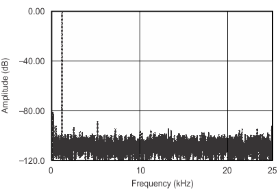 Figure 2. Frequency Spectrum
 (4096 Point FFT: fIN = 1 kHz, 0 dB)
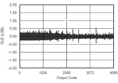 Figure 4. Differential Linearity Error vs Code
 (2.5-V Internal Reference)
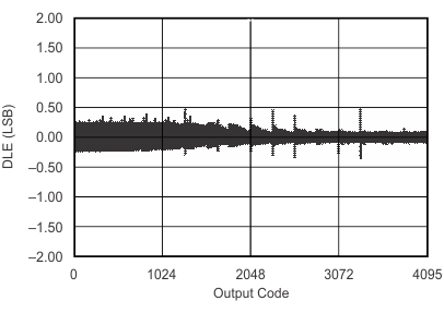 Figure 6. Differential Linearity Error vs Code
 (2.5-V External Reference)
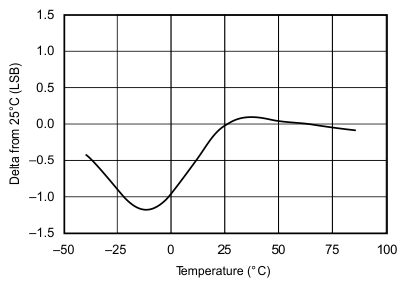 Figure 8. Change in Gain vs Temperature
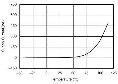 Figure 10. Power-Down Supply Current vs Temperature
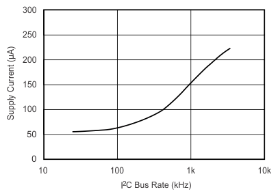 Figure 12. Supply Current vs I2C Bus Rate
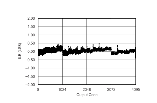 Figure 3. Integral Linearity Error vs Code
 (2.5-V Internal Reference)
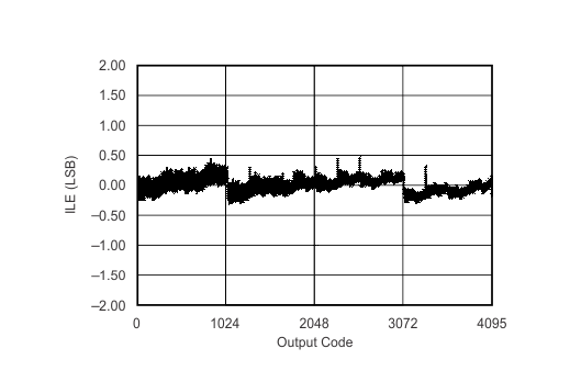 Figure 5. Integral Linearity Error vs Code
 (2.5-V External Reference)
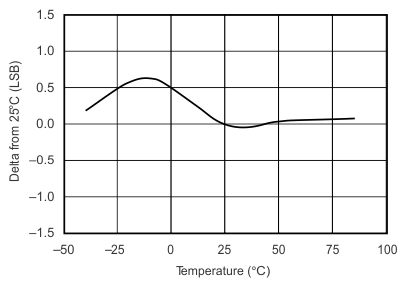 Figure 7. Change in Offset vs Temperature
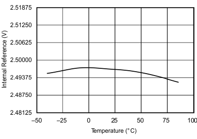 Figure 9. Internal Reference vs Temperature
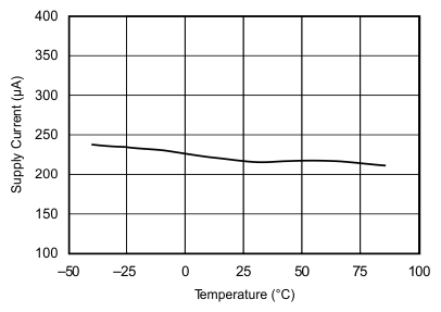 Figure 11. Supply Current vs Temperature
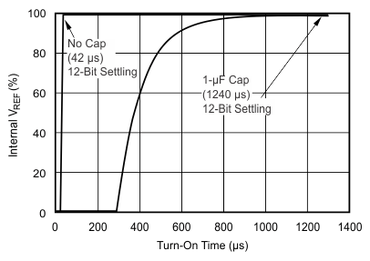 Figure 13. Internal VREF vs Turn-On Time