SLAS708A September 2010 – September 2019 ADS7947 , ADS7948 , ADS7949
PRODUCTION DATA.
- 1 Features
- 2 Applications
- 3 Description
- 4 Revision History
- 5 Device Comparison Table
- 6 Pin Configuration and Functions
-
7 Specifications
- 7.1 Absolute Maximum Ratings
- 7.2 ESD Ratings
- 7.3 Recommended Operating Conditions: ADS794x (12-, 10-, 8-Bit)
- 7.4 Thermal Information
- 7.5 Electrical Characteristics: ADS7947 (12-Bit)
- 7.6 Electrical Characteristics: ADS7948 (10-Bit)
- 7.7 Electrical Characteristics: ADS7949 (8-Bit)
- 7.8 Timing Requirements
- 7.9 Switching Characteristics
- 7.10 Typical Characteristics: ADS7947, ADS7948, ADS7949
- 7.11 Typical Characteristics: ADS7947 (12-Bit)
- 8 Detailed Description
- 9 Application and Implementation
- 10Power Supply Recommendations
- 11Layout
- 12Device and Documentation Support
- 13Mechanical, Packaging, and Orderable Information
Package Options
Mechanical Data (Package|Pins)
- RTE|16
Thermal pad, mechanical data (Package|Pins)
- RTE|16
Orderable Information
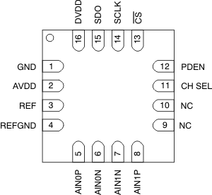
6 Pin Configuration and Functions
RTE Package
16-Pin WQFN
Top View

Pin Functions
| PIN NO. | PIN NAME | FUNCTION | DESCRIPTION |
|---|---|---|---|
| 1 | GND | Analog/digital | Power supply ground; all analog and digital signals are referred with respect to this pin. |
| 2 | AVDD | Analog | ADC power supply. |
| 3 | REF | Analog | ADC positive reference input; decouple this pin with REFGND. |
| 4 | REFGND | Analog | Reference return; short to analog ground plane. |
| 5 | AIN0P | Analog input | Positive analog input, channel 0. |
| 6 | AIN0N | Analog input | Negative analog input, channel 0. The allowable signal swing on this pin is ±0.2V; this pin can be grounded. |
| 7 | AIN1N | Analog input | Negative analog input, channel 1. The allowable signal swing on this pin is ±0.2V; this pin can be grounded. |
| 8 | AIN1P | Analog input | Positive analog input, channel 1. |
| 9 | NC | — | Not connected internally, TI recommends externally shorting this pin to GND. |
| 10 | NC | — | Not connected internally, TI recommends externally shorting this pin to GND. |
| 11 | CH SEL | Digital input | This pin selects the analog input channel.
Low = channel 0, high = channel 1. TI recommends changing the channel within a window of one clock; from half a clock after the CS falling edge. This change ensures the settling on the multiplexer output before the sample start. |
| 12 | PDEN | Digital input | This pin enables a power-down feature if this pin is high at the CS rising edge. |
| 13 | CS | Digital input | Chip-select signal; active low. |
| 14 | SCLK | Digital input | Serial SPI clock. |
| 15 | SDO | Digital output | Serial data out. |
| 16 | DVDD | Digital | Digital I/O supply. |