SLAS605C June 2008 – July 2018 ADS7950 , ADS7951 , ADS7952 , ADS7953 , ADS7954 , ADS7955 , ADS7956 , ADS7957 , ADS7958 , ADS7959 , ADS7960 , ADS7961
PRODUCTION DATA.
- 1 Features
- 2 Applications
- 3 Description
- 4 Revision History
- 5 Device Comparison Table
- 6 Pin Configuration and Functions
-
7 Specifications
- 7.1 Absolute Maximum Ratings
- 7.2 ESD Ratings
- 7.3 Recommended Operating Conditions
- 7.4 Thermal Information: TSSOP
- 7.5 Thermal Information: VQFN
- 7.6 Electrical Characteristics: ADS7950, ADS7951, ADS7952, ADS7953
- 7.7 Electrical Characteristics, ADS7954, ADS7955, ADS7956, ADS7957
- 7.8 Electrical Characteristics, ADS7958, ADS7959, ADS7960, ADS7961
- 7.9 Timing Requirements
- 7.10 Typical Characteristics (All ADS79xx Family Devices)
- 7.11 Typical Characteristics (12-Bit Devices Only)
- 7.12 Typical Characteristics (12-Bit Devices Only)
- 8 Detailed Description
- 9 Application and Implementation
- 10Power Supply Recommendations
- 11Layout
- 12Device and Documentation Support
- 13Mechanical, Packaging, and Orderable Information
Package Options
Refer to the PDF data sheet for device specific package drawings
Mechanical Data (Package|Pins)
- RHB|32
- DBT|38
Thermal pad, mechanical data (Package|Pins)
- RHB|32
Orderable Information
8.5.2 GPIO Registers
NOTE
GPIO 0, 1, 2, and 3 are available in the TSSOP packages. Only GPIO 0 is available in the VQFN packages.
The device has four general purpose input and output (GPIO) pins. Each of the four pins can be independently programmed as general purpose output (GPO) or general purpose input (GPI). It is also possible to use the GPIOs for some pre-assigned functions (refer to Table 11 for details). GPO data can be written into the device through the SDI line. The device refreshes the GPO data on every CS falling edge as per the SDI data written in the previous frame. Similarly, the device latches GPI status on the CS falling edge and outputs it on SDO (if GPI is read enabled by writing DI04 = 1 during the previous frame) in the same frame starting on the CS falling edge.
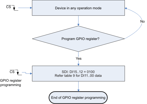
The details regarding programming the GPIO registers are illustrated in the flowchart in Figure 58. Table 11 lists the details regarding GPIO Register programming settings.

NOTE:
The device continues its operation in selected mode during programming. SDO is valid, however it is not possible to change the range or write GPIO data into the device during programming.Table 11. GPIO Program Register Settings
| BITS | RESET STATE | LOGIC STATE | FUNCTION |
|---|---|---|---|
| DI15-12 | NA | 0100 | Device selects GPIO Program Registers for programming. |
| DI11-10 | 00 | 00 | Do not program these bits to any logic state other than ‘00’ |
| DI09 | 0 | 1 | Device resets all registers in the next CS frame to the reset state shown in the corresponding tables (it also resets itself). |
| 0 | Device normal operation | ||
| DI08 | 0 | 1 | Device configures GPIO3 as the device power-down input. |
| 0 | GPIO3 remains general purpose I or O. Program 0 for QFN packaged devices. | ||
| DI07 | 0 | 1 | Device configures GPIO2 as device range input. |
| 0 | GPIO2 remains general purpose I or O. Program 0 for QFN packaged devices. | ||
| DI06-04 | 000 | 000 | GPIO1 and GPIO0 remain general purpose I or O. Valid setting for QFN packaged devices. |
| xx1 | Device configures GPIO0 as ‘high or low’ alarm output. This is an active high output. GPIO1 remains general purpose I or O. Valid setting for QFN packaged devices. | ||
| 010 | Device configures GPIO0 as high alarm output. This is an active high output. GPIO1 remains general purpose I or O. Valid setting for QFN packaged devices. | ||
| 100 | Device configures GPIO1 as low alarm output. This is an active high output. GPIO0 remains general purpose I or O. Setting not allowed for QFN packaged devices. | ||
| 110 | Device configures GPIO1 as low alarm output and GPIO0 as a high alarm output. These are active high outputs. Setting not allowed for QFN packaged devices. | ||
| Note: The following settings are valid for GPIO which are not assigned a specific function through bits DI08..04 | |||
| DI03 | 0 | 1 | GPIO3 pin is configured as general purpose output. Program 1 for QFN packaged devices. |
| 0 | GPIO3 pin is configured as general purpose input. Setting not allowed for QFN packaged devices. | ||
| DI02 | 0 | 1 | GPIO2 pin is configured as general purpose output. Program 1 for QFN packaged devices. |
| 0 | GPIO2 pin is configured as general purpose input. Setting not allowed for QFN packaged devices. | ||
| DI01 | 0 | 1 | GPIO1 pin is configured as general purpose output. Program 1 for QFN packaged devices. |
| 0 | GPIO1 pin is configured as general purpose input. Setting not allowed for QFN packaged devices. | ||
| DI00 | 0 | 1 | GPIO0 pin is configured as general purpose output. Valid setting for QFN packaged devices. |
| 0 | GPIO0 pin is configured as general purpose input. Valid setting for QFN packaged devices. | ||