SLAS605C June   2008  – July 2018 ADS7950 , ADS7951 , ADS7952 , ADS7953 , ADS7954 , ADS7955 , ADS7956 , ADS7957 , ADS7958 , ADS7959 , ADS7960 , ADS7961

PRODUCTION DATA.  

  1. Features
  2. Applications
    1.     Detailed Block Diagram
  3. Description
  4. Revision History
  5. Device Comparison Table
  6. Pin Configuration and Functions
    1.     Pin Functions: TSSOP Packages
    2.     Pin Functions: VQFN Packages
  7. Specifications
    1. 7.1  Absolute Maximum Ratings
    2. 7.2  ESD Ratings
    3. 7.3  Recommended Operating Conditions
    4. 7.4  Thermal Information: TSSOP
    5. 7.5  Thermal Information: VQFN
    6. 7.6  Electrical Characteristics: ADS7950, ADS7951, ADS7952, ADS7953
    7. 7.7  Electrical Characteristics, ADS7954, ADS7955, ADS7956, ADS7957
    8. 7.8  Electrical Characteristics, ADS7958, ADS7959, ADS7960, ADS7961
    9. 7.9  Timing Requirements
    10. 7.10 Typical Characteristics (All ADS79xx Family Devices)
    11. 7.11 Typical Characteristics (12-Bit Devices Only)
    12. 7.12 Typical Characteristics (12-Bit Devices Only)
  8. Detailed Description
    1. 8.1 Overview
    2. 8.2 Functional Block Diagram
    3. 8.3 Feature Description
      1. 8.3.1 Reference
      2. 8.3.2 Power Saving
    4. 8.4 Device Functional Modes
      1. 8.4.1 Channel Sequencing Modes
      2. 8.4.2 Device Programming and Mode Control
        1. 8.4.2.1 Mode Control Register
        2. 8.4.2.2 Program Registers
      3. 8.4.3 Device Power-Up Sequence
      4. 8.4.4 Operating in Manual Mode
      5. 8.4.5 Operating in Auto-1 Mode
      6. 8.4.6 Operating in Auto-2 Mode
      7. 8.4.7 Continued Operation in a Selected Mode
    5. 8.5 Programming
      1. 8.5.1 Digital Output
      2. 8.5.2 GPIO Registers
      3. 8.5.3 Alarm Thresholds for GPIO Pins
  9. Application and Implementation
    1. 9.1 Application Information
      1. 9.1.1 Analog Input
    2. 9.2 Typical Applications
      1. 9.2.1 Unbuffered Multiplexer Output (MXO)
        1. 9.2.1.1 Design Requirements
        2. 9.2.1.2 Detailed Design Procedure
        3. 9.2.1.3 Application Curves
      2. 9.2.2 OPA192 Buffered Multiplexer Output (MXO)
        1. 9.2.2.1 Design Requirements
        2. 9.2.2.2 Detailed Design Procedure
        3. 9.2.2.3 Application Curves
  10. 10Power Supply Recommendations
  11. 11Layout
    1. 11.1 Layout Guidelines
    2. 11.2 Layout Examples
  12. 12Device and Documentation Support
    1. 12.1 Documentation Support
      1. 12.1.1 Related Documentation
    2. 12.2 Related Links
    3. 12.3 Receiving Notification of Documentation Updates
    4. 12.4 Community Resources
    5. 12.5 Trademarks
    6. 12.6 Electrostatic Discharge Caution
    7. 12.7 Glossary
  13. 13Mechanical, Packaging, and Orderable Information

Package Options

Refer to the PDF data sheet for device specific package drawings

Mechanical Data (Package|Pins)
  • RHB|32
  • DBT|38
Thermal pad, mechanical data (Package|Pins)
Orderable Information

OPA192 Buffered Multiplexer Output (MXO)

The use of a buffer relaxes the RSOURCE requirements to an extent. Charge from the sample-and-hold capacitor no longer dominates as a residual charge from a previous channel. Although having good performance is possible with a larger impedance using the OPA192, the output capacitance of the MXO also holds the previous channel charge and cannot be isolated, which limits how large the input impedance can finally be for good performance. In this configuration, the 1xVREF range allows slightly higher impedance because the OPA192 (20 V/µs) slews approximately 2.5 V in contrast to the 2xVREF range that requires the OPA192 to slew approximately 5 V.
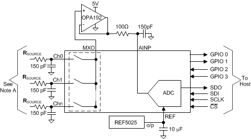
ADS7950 ADS7951 ADS7952 ADS7953 ADS7954 ADS7955 ADS7956 ADS7957 ADS7958 ADS7959 ADS7960 ADS7961 apps_OPA192.gif
Restriction on the source impedance exists. R(SOURCE) ≤ 500 Ω for a 12-bit settling at 1 MSPS with both 1xVREF and 2xVREF ranges.
Figure 66. Application Diagram for an OPA192 Buffered MXO