SBAS817D November 2017 – June 2024 ADS8166 , ADS8167 , ADS8168
PRODUCTION DATA
- 1
- 1 Features
- 2 Applications
- 3 Description
- 4 Pin Configuration and Functions
- 5 Specifications
- 6 Detailed Description
-
7 Register Maps
- 7.1
Interface and Hardware Configuration Registers
- 7.1.1 REG_ACCESS Register (address = 00h) [reset = 00h]
- 7.1.2 PD_CNTL Register (address = 04h) [reset = 00h]
- 7.1.3 SDI_CNTL Register (address = 008h) [reset = 00h]
- 7.1.4 SDO_CNTL1 Register (address = 0Ch) [reset = 00h]
- 7.1.5 SDO_CNTL2 Register (address = 0Dh) [reset = 00h]
- 7.1.6 SDO_CNTL3 Register (address = 0Eh) [reset = 00h]
- 7.1.7 SDO_CNTL4 Register (address = 0Fh) [reset = 00h]
- 7.1.8 DATA_CNTL Register (address = 10h) [reset = 00h]
- 7.1.9 PARITY_CNTL Register (address = 11h) [reset = 00h]
- 7.2 Device Calibration Registers
- 7.3 Analog Input Configuration Registers
- 7.4
Channel Sequence Configuration Registers Map
- 7.4.1 DEVICE_CFG Register (address = 1Ch) [reset = 00h]
- 7.4.2 CHANNEL_ID Register (address = 1Dh) [reset = 00h]
- 7.4.3 SEQ_START Register (address = 1Eh) [reset = 00h]
- 7.4.4 SEQ_ABORT Register (address = 1Fh) [reset = 00h]
- 7.4.5 ON_THE_FLY_CFG Register (address = 2Ah) [reset = 00h]
- 7.4.6 AUTO_SEQ_CFG1 Register (address = 80h) [reset = 00h]
- 7.4.7 AUTO_SEQ_CFG2 Register (address = 82h) [reset = 00h]
- 7.4.8
Custom Channel Sequencing Mode Registers
- 7.4.8.1 CCS_START_INDEX Register (address = 88h) [reset = 00h]
- 7.4.8.2 CCS_END_INDEX Register (address = 89h) [reset = 00h]
- 7.4.8.3 CCS_SEQ_LOOP Register (address = 8Ah) [reset = 00h]
- 7.4.8.4 CCS_CHID_INDEX_m Registers (address = 8C, 8E, 90, 92, 94, 96, 98, 9A, 9C, 9E, A0, A2, A4, A6, A8, and AAh) [reset = 00h]
- 7.4.8.5 REPEAT_INDEX_m Registers (address = 8D, 8F, 91, 93, 95, 97, 99, 9B, 9D, 9F, A1, A3, A5, A7, A9, and ABh) [reset = 00h]
- 7.5
Digital Window Comparator Configuration Registers Map
- 7.5.1 ALERT_CFG Register (address = 2Eh) [reset = 00h]
- 7.5.2 HI_TRIG_AINx[15:0] Register (address = 4Dh to 30h) [reset = 0000h]
- 7.5.3 LO_TRIG_AINx[15:0] Register (address = 71h to 54h) [reset = 0000h]
- 7.5.4 HYSTERESIS_AINx[7:0] Register (address = 4Fh to 33h) [reset = 00h]
- 7.5.5 ALERT_LO_STATUS Register (address = 78h) [reset = 00h]
- 7.5.6 ALERT_HI_STATUS Register (address = 79h) [reset = 00h]
- 7.5.7 ALERT_STATUS Register (address = 7Ah) [reset = 00h]
- 7.5.8 CURR_ALERT_LO_STATUS Register (address = 7Ch) [reset = 00h]
- 7.5.9 CURR_ALERT_HI_STATUS Register (address = 7Dh) [reset = 00h]
- 7.5.10 CURR_ALERT_STATUS Register (address = 7Eh) [reset = 00h]
- 7.1
Interface and Hardware Configuration Registers
- 8 Application and Implementation
- 9 Device and Documentation Support
- 10Revision History
- 11Mechanical, Packaging, and Orderable Information
Package Options
Mechanical Data (Package|Pins)
- RHB|32
Thermal pad, mechanical data (Package|Pins)
- RHB|32
Orderable Information
5.8 Timing Diagrams

A. The SPI-00 interface mode is
illustrated here. For SPI-01, -10, and-11 modes, see the Enhanced-SPI Interface section.
Figure 5-1 Conversion Cycle Timing: CS = 1 Longer Than
tCONV
A. The SPI-00 interface mode is
illustrated here. For SPI-01, -10, and-11 modes, see the Enhanced-SPI Interface section.
Figure 5-2 Conversion Cycle Timing: CS = 1 Shorter Than
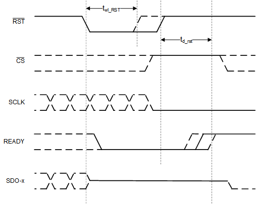
tCONV Figure 5-3 Asynchronous Reset Timing
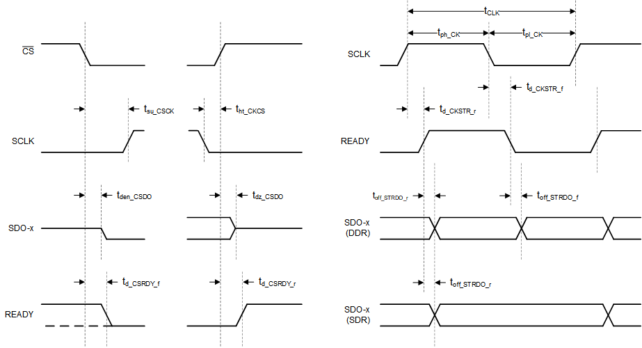
 Figure 5-4 Clock
Re-Timer Serial Interface Timing