SBAS817D November 2017 – June 2024 ADS8166 , ADS8167 , ADS8168
PRODUCTION DATA
- 1
- 1 Features
- 2 Applications
- 3 Description
- 4 Pin Configuration and Functions
- 5 Specifications
- 6 Detailed Description
-
7 Register Maps
- 7.1
Interface and Hardware Configuration Registers
- 7.1.1 REG_ACCESS Register (address = 00h) [reset = 00h]
- 7.1.2 PD_CNTL Register (address = 04h) [reset = 00h]
- 7.1.3 SDI_CNTL Register (address = 008h) [reset = 00h]
- 7.1.4 SDO_CNTL1 Register (address = 0Ch) [reset = 00h]
- 7.1.5 SDO_CNTL2 Register (address = 0Dh) [reset = 00h]
- 7.1.6 SDO_CNTL3 Register (address = 0Eh) [reset = 00h]
- 7.1.7 SDO_CNTL4 Register (address = 0Fh) [reset = 00h]
- 7.1.8 DATA_CNTL Register (address = 10h) [reset = 00h]
- 7.1.9 PARITY_CNTL Register (address = 11h) [reset = 00h]
- 7.2 Device Calibration Registers
- 7.3 Analog Input Configuration Registers
- 7.4
Channel Sequence Configuration Registers Map
- 7.4.1 DEVICE_CFG Register (address = 1Ch) [reset = 00h]
- 7.4.2 CHANNEL_ID Register (address = 1Dh) [reset = 00h]
- 7.4.3 SEQ_START Register (address = 1Eh) [reset = 00h]
- 7.4.4 SEQ_ABORT Register (address = 1Fh) [reset = 00h]
- 7.4.5 ON_THE_FLY_CFG Register (address = 2Ah) [reset = 00h]
- 7.4.6 AUTO_SEQ_CFG1 Register (address = 80h) [reset = 00h]
- 7.4.7 AUTO_SEQ_CFG2 Register (address = 82h) [reset = 00h]
- 7.4.8
Custom Channel Sequencing Mode Registers
- 7.4.8.1 CCS_START_INDEX Register (address = 88h) [reset = 00h]
- 7.4.8.2 CCS_END_INDEX Register (address = 89h) [reset = 00h]
- 7.4.8.3 CCS_SEQ_LOOP Register (address = 8Ah) [reset = 00h]
- 7.4.8.4 CCS_CHID_INDEX_m Registers (address = 8C, 8E, 90, 92, 94, 96, 98, 9A, 9C, 9E, A0, A2, A4, A6, A8, and AAh) [reset = 00h]
- 7.4.8.5 REPEAT_INDEX_m Registers (address = 8D, 8F, 91, 93, 95, 97, 99, 9B, 9D, 9F, A1, A3, A5, A7, A9, and ABh) [reset = 00h]
- 7.5
Digital Window Comparator Configuration Registers Map
- 7.5.1 ALERT_CFG Register (address = 2Eh) [reset = 00h]
- 7.5.2 HI_TRIG_AINx[15:0] Register (address = 4Dh to 30h) [reset = 0000h]
- 7.5.3 LO_TRIG_AINx[15:0] Register (address = 71h to 54h) [reset = 0000h]
- 7.5.4 HYSTERESIS_AINx[7:0] Register (address = 4Fh to 33h) [reset = 00h]
- 7.5.5 ALERT_LO_STATUS Register (address = 78h) [reset = 00h]
- 7.5.6 ALERT_HI_STATUS Register (address = 79h) [reset = 00h]
- 7.5.7 ALERT_STATUS Register (address = 7Ah) [reset = 00h]
- 7.5.8 CURR_ALERT_LO_STATUS Register (address = 7Ch) [reset = 00h]
- 7.5.9 CURR_ALERT_HI_STATUS Register (address = 7Dh) [reset = 00h]
- 7.5.10 CURR_ALERT_STATUS Register (address = 7Eh) [reset = 00h]
- 7.1
Interface and Hardware Configuration Registers
- 8 Application and Implementation
- 9 Device and Documentation Support
- 10Revision History
- 11Mechanical, Packaging, and Orderable Information
Package Options
Mechanical Data (Package|Pins)
- RHB|32
Thermal pad, mechanical data (Package|Pins)
- RHB|32
Orderable Information
6.3.1.1 Multiplexer Configurations
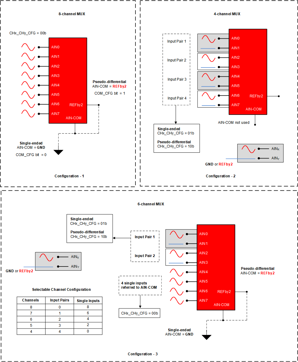
The ADS816x supports single-ended and pseudo-differential analog input signals. The flexible analog input channel configuration supports interfacing various types of sensors. Figure 6-2 shows how different configurations for the analog inputs.
 Figure 6-2 Analog Input Configurations
The analog inputs configurations are:
- Configuration 1: Eight-channel MUX with the AIN_CFG register set to 00h. The AIN-COM input range is decided by
the COM_CFG register.
- Single-ended inputs with the AIN-COM input set to GND (set the COM_CFG register to 00h).
- Pseudo-differential inputs with the AIN-COM input set to VREF / 2 (set the COM_CFG register to 01h).
- Configuration 2: Four-channel MUX.
- As shown in Table 6-1, the AIN_CFG register selects the analog input range of individual pairs.
- Configuration 3: Single-ended and pseudo-differential inputs.
- Among the eight analog inputs of the MUX, some inputs are configured as pairs and some inputs are configured as individual channels. Table 6-1 lists options for channel configuration.
- For channels configured as pairs, the AIN_CFG register selects the single-ended or pseudo-differential configuration for individual pairs.
- For individual channels, the COM_CFG register decides the single-ended or pseudo-differential configuration.
| SERIAL NUMBER | TOTAL CHANNELS | INPUT PAIRS(1)(2) | INDIVIDUAL CHANNELS |
|---|---|---|---|
| 1 | 8 | 0 | 8 |
| 2 | 7 | 1 | 6 |
| 3 | 6 | 2 | 4 |
| 4 | 5 | 3 | 2 |
| 5 | 4 | 4 | 0 |
The COM_CFG register sets the input voltage range of the AIN-COM pin. Connect the AIN-COM pin to GND (set the COM_CFG register to 0b) or REFby2 (set the COM_CFG register to 1b) externally. When using the MUX in a four-channel configuration, the COM_CFG register has no effect; connect the AIN-COM pin to GND to avoid noise coupling.