SBAS108E May 2000 – December 2016 ADS8320
PRODUCTION DATA.
- 1 Features
- 2 Applications
- 3 Description
- 4 Revision History
- 5 Pin Configuration and Functions
- 6 Specifications
- 7 Detailed Description
- 8 Application and Implementation
- 9 Power Supply Recommendations
- 10Layout
- 11Device and Documentation Support
- 12Mechanical, Packaging, and Orderable Information
Package Options
Mechanical Data (Package|Pins)
- DGK|8
Thermal pad, mechanical data (Package|Pins)
Orderable Information
10 Layout
10.1 Layout Guidelines
For optimum performance, care must be taken with the physical layout of the ADS8320 circuitry. This is particularly true if the reference voltage is low and/or the conversion rate is high. At a 100-kHz conversion rate, the ADS8320 makes a bit decision every 416 ns. That is, for each subsequent bit decision, the digital output must be updated with the results of the last bit decision, the capacitor array appropriately switched and charged, and the input to the comparator settled to a 16-bit level all within one clock cycle.
TI recommends following these layout guidelines:
- A printed-circuit board (PCB) with at least four layers to keep all critical components on the top layer.
- Analog input signals and the reference input signals must be kept away from noise sources. Crossing digital lines with the analog signal path must be avoided. The analog input and the reference signals are routed on to the left side of the board and the digital connections are routed on the right side of the device.
- Due to the dynamic currents that occur during conversion and data transfer, the supply pin (+VCC) must have a decoupling capacitor that keeps the supply voltage stable. A 1-µF ceramic decoupling capacitor is recommended for the supply pin.
- A layout that interconnects the converter and accompanying capacitors with the low inductance path is critical for achieving optimal performance. Using 15-mil vias to interconnect components to a solid analog ground plane at the subsequent inner layer minimizes stray inductance. Avoid placing vias between the supply pin and the decoupling capacitor. Any inductance between the supply capacitor and the supply pin of the converter must be kept to less than 5 nH by placing the capacitor within 0.2 inches from the supply or input pins of the ADS8320 and by using 20-mil traces.
- Dynamic currents are also present at the REF pin during the conversion phase. Therefore, good decoupling is critical to achieve optimal performance. The inductance between the reference capacitor and the REF pin must be kept to less than 2 nH by placing the capacitor within 0.1 inches from the REFIN pin and by using 20-mil traces.
- A single 10-µF, X7R-grade, 0805-size ceramic capacitor with at least a 10-V rating for good performance over temperature range.
- A small, 0.1-Ω to 0.47-Ω, 0603-size resistor placed in series with the reference capacitor keeps the overall impedance low and constant, especially at very high frequencies.
- Avoid using additional lower value capacitors because the interactions between multiple capacitors can affect the ADC performance at higher sampling rates.
- Place the RC filters immediately next to the input pins. Among surface-mount capacitors, COG (NPO) ceramic capacitors provide the best capacitance precision. The type of dielectric used in COG (NPO) ceramic capacitors provides the most stable electrical properties over voltage, frequency, and temperature changes.
- The GND pin on the ADS8320 must be placed on a clean ground plane. In many cases, this is the analog ground.
10.2 Layout Example
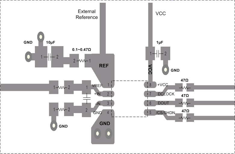 Figure 28. Layout Example
10.3 Power Dissipation
The architecture of the converter, the semiconductor fabrication process, and a careful design allow the ADS8320 to convert at up to a 100kHz rate while requiring very little power. Still, for the absolute lowest power dissipation, there are several things to keep in mind.
The power dissipation of the ADS8320 scales directly with conversion rate. Therefore, the first step to achieving the lowest power dissipation is to find the lowest conversion rate that satisfies the requirements of the system.
In addition, the ADS8320 is in power-down mode under two conditions: when the conversion is complete and whenever CS is HIGH (as shown in Figure 29). Ideally, each conversion must occur as quickly as possible, preferably at a 2.4-MHz clock rate. This way, the converter spends the longest possible time in the power-down mode. This is very important as the converter not only uses power on each DCLOCK transition (as is typical for digital CMOS components), but also uses some current for the analog circuitry, such as the comparator. The analog section dissipates power continuously, until the power-down mode is entered.
The following timing diagrams and test circuits pertain to the parameters in Table 1.

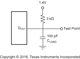 Figure 30. Load Circuit for tdDO, tr, and tf
 Figure 31. Voltage Waveforms for DOUT Rise and Fall Times, tr, tf
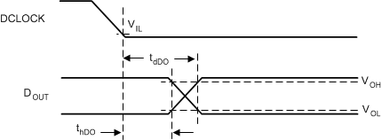 Figure 32. Voltage Waveforms for DOUT Delay Times, tdDO
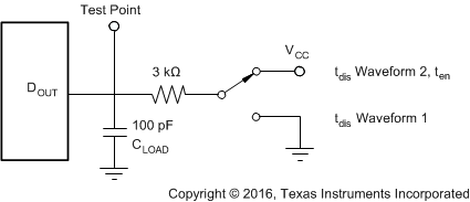
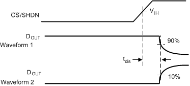 Figure 34. Voltage Waveforms for tdis
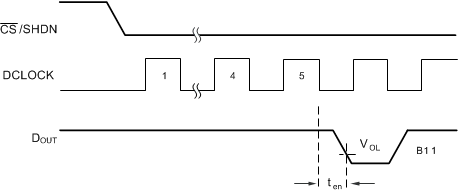 Figure 35. Voltage Waveforms for ten
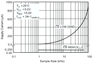
Figure 36 shows the current consumption of the ADS8320 versus sample rate. For this graph, the converter is clocked at 2.4 MHz regardless of the sample rate; CS is HIGH for the remaining sample period. Figure 37 also shows current consumption versus sample rate. However, in this case, the DCLOCK period is 1/24th of the sample period—CS is HIGH for one DCLOCK cycle out of every 16.
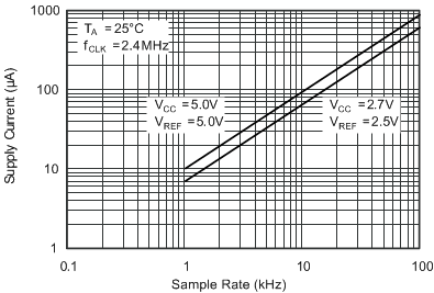 Figure 36. Maintaining fCLK at the Highest Possible Rate Allows Supply Current to Drop Linearly With Sample Rate
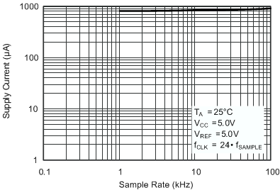 Figure 37. Scaling fCLK Reduces Supply Current Only Slightly With Sample Rate
There is an important distinction between the power-down mode that is entered after a conversion is complete and the full power-down mode which is enabled when CS is HIGH. CS LOW shuts down only the analog section. The digital section is completely shut down only when CS is HIGH. Thus, if CS is left LOW at the end of a conversion and the converter is continually clocked, the power consumption is not as low as when CS is HIGH. Figure 38 shows more information.
Power dissipation can also be reduced by lowering the power-supply voltage and the reference voltage. The ADS8320 operates over a VCC range of 2 V to 5.25 V. However, at voltages below 2.7 V, the converter does not run at a 100-kHz sample rate. See Typical Characteristics for more information regarding power supply voltage and maximum sample rate.
10.3.1 Short Cycling
Another way of saving power is to use the CS signal to short cycle the conversion. Because the ADS8320 places the latest data bit on the DOUT line as it is generated, the converter can easily be short cycled. This term means that the conversion can be terminated at any time. For example, if only 14 bits of the conversion result are required, then the conversion can be terminated (by pulling CS HIGH) after the 14th bit has been clocked out.
This technique can be used to lower the power dissipation (or to increase the conversion rate) in those applications where an analog signal is being monitored until some condition becomes true. For example, if the signal is outside a predetermined range, the full 16-bit conversion result may not be required. If so, the conversion can be terminated after the first n bits, where n might be as low as 3 or 4. This results in lower power dissipation in both the converter and the rest of the system, as they spend more time in the power-down mode.