SBAS761A February 2020 – February 2020 ADS8355
PRODUCTION DATA.
- 1 Features
- 2 Applications
- 3 Description
- 4 Revision History
- 5 Pin Configuration and Functions
- 6 Specifications
-
7 Detailed Description
- 7.1 Overview
- 7.2 Functional Block Diagram
- 7.3 Feature Description
- 7.4 Device Functional Modes
- 7.5 Programming
- 7.6
Register Map
- 7.6.1
ADS8355 Registers
- 7.6.1.1 PD_STANDBY Register (Offset = 4h) [reset = 0h]
- 7.6.1.2 PD_KEY Register (Offset = 5h) [reset = 0h]
- 7.6.1.3 SDO_CTRL Register (Offset = Dh) [reset = 0h]
- 7.6.1.4 DATA_OUT_CTRL Register (Offset = 11h) [reset = 0h]
- 7.6.1.5 REF_SEL Register (Offset = 20h) [reset = 0h]
- 7.6.1.6 REFDAC_A_LSB Register (Offset = 24h) [reset = 0h]
- 7.6.1.7 REFDAC_A_MSB Register (Offset = 25h) [reset = 0h]
- 7.6.1.8 REFDAC_B_LSB Register (Offset = 26h) [reset = 0h]
- 7.6.1.9 REFDAC_B_MSB Register (Offset = 27h) [reset = 0h]
- 7.6.1.10 INPUT_CONFIG Register (Offset = 28h) [reset = 0h]
- 7.6.1
ADS8355 Registers
- 8 Application and Implementation
- 9 Power Supply Recommendations
- 10Layout
- 11Device and Documentation Support
- 12Mechanical, Packaging, and Orderable Information
Package Options
Mechanical Data (Package|Pins)
- RTE|16
Thermal pad, mechanical data (Package|Pins)
- RTE|16
Orderable Information
7.3.1 Reference
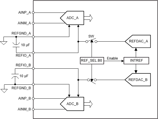
The device has two simultaneous sampling ADCs: ADC_A and ADC_B. ADC_A and ADC_B operate with reference voltages VREF_A and VREF_B present on the REFIO_A and REFIO_B pins, respectively. Decouple the REFIO_A and REFIO_B pins with the REFGND_A and REFGND_B pins, respectively, with 10-µF decoupling capacitors.
As illustrated in Figure 24, the device supports operation either with an internal or external reference source. The reference voltage source is determined by programming the INT_EXT bit of the REF_SEL register. This bit is common to ADC_A and ADC_B.
 Figure 24. Reference Configurations and Connections
 The default value of the REF_SEL register bit INT_EXT is set to 0. The device ADC_A and ADC_B operate with the external reference voltages provided on the REFIO_A and REFIO_B pins, respectively.
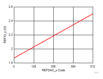
When the REF_SEL register bit INT_EXT is set to 1, the device operates with the internal reference source connected to REFIO_A and REFIO_B. The individual reference voltages can be set independently by programming the REFDAC_A and REFDAC_B values, respectively. For a 2.5-V internal reference, program REFDAC_x with a 0x1FF value..
Figure 25 shows a typical transfer function for the internal REFDAC when the internal reference is enabled.
 Figure 25. REFDAC Transfer Function