SBAS531D December 2010 – February 2016 ADS8555
PRODUCTION DATA.
- 1 Features
- 2 Applications
- 3 Description
- 4 Revision History
- 5 Pin Configuration and Functions
-
6 Specifications
- 6.1 Absolute Maximum Ratings
- 6.2 ESD Ratings
- 6.3 Recommended Operating Conditions
- 6.4 Thermal Information
- 6.5 Electrical Characteristics
- 6.6 Serial Interface Timing Requirements
- 6.7 Parallel Interface Timing Requirements (Read Access)
- 6.8 Parallel Interface Timing Requirements (Write Access)
- 6.9 Typical Characteristics
- 7 Detailed Description
- 8 Applications and Implementation
- 9 Power Supply Recommendations
- 10Layout
- 11Device and Documentation Support
- 12Mechanical, Packaging, and Orderable Information
Package Options
Mechanical Data (Package|Pins)
- PM|64
Thermal pad, mechanical data (Package|Pins)
Orderable Information
7 Detailed Description
7.1 Overview
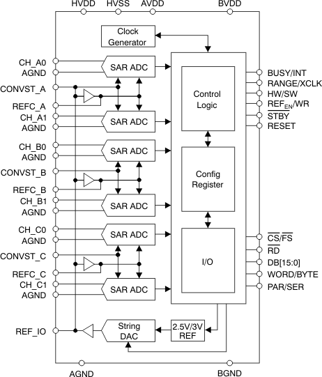
The ADS8555 device includes six 16-bit analog-to-digital converters (ADCs) that operate based on the successive approximation register (SAR) principle. The architecture is designed on the charge redistribution principle that inherently includes a sample-and-hold function. The six analog inputs are grouped into three channel pairs. These channel pairs can be sampled and converted simultaneously, preserving the relative phase information of the signals of each pair. Separate conversion start signals allow simultaneous sampling on each channel pair, on four channels or on all six channels.
These devices accept single-ended, bipolar analog input signals in the selectable ranges of ±4 VREF or ±2 VREF with an absolute value of up to ±12 V; see the Analog Inputs section for more details.
The devices offer an internal 2.5-V, 3-V reference source followed by a 10-bit, digital-to-analog converter (DAC) that allows the reference voltage VREF to be adjusted in 2.44-mV or 2.93-mV steps, respectively.
The ADS8555 device also offers a selectable parallel or serial interface that can be used in hardware or software mode; see the Device Configuration section for details.
7.2 Functional Block Diagram
7.3 Feature Description
7.3.1 Analog
This section addresses the analog input circuit, the ADCs and control signals, and the reference design of the device.
7.3.1.1 Analog Inputs
The inputs and the converters are of the single-ended, bipolar type. The absolute voltage range can be selected using the RANGE pin (in hardware mode) or RANGE_x bits (in software mode) in the control register (CR, see Table 5) to either ±4 VREF or ±2 VREF. With the reference set to 2.5 V (CR bit C18 = 0), the input voltage range can be ±10 V or ±5 V. With the reference source set to 3 V (CR bit C18 = 1), an input voltage range of ±12 V or ±6 V can be configured. The logic state of the RANGE pin is latched with the falling edge of BUSY (if CR bit C20 = 0).
The input current on the analog inputs depends on the actual sample rate, input voltage, and signal source impedance. Essentially, the current into the analog inputs charges the internal capacitor array only during the sampling period (tACQ). The source of the analog input voltage must be able to charge the input capacitance of 10 pF in ±4-VREF mode or 20 pF in ±2-VREF mode to a 12-, 14-, 16-bit accuracy level within the acquisition time of 280 ns at maximum data rate, as shown in Figure 29.
 Figure 29. Equivalent Input Circuits
During the conversion period, there is no further input current flow and the input impedance is greater than 1 MΩ. To ensure a defined start condition, the sampling capacitors of the ADS8555 device are precharged to a fixed internal voltage, before switching into sampling mode.
To maintain the linearity of the converter, the inputs must always remain within the specified range of HVSS – 0.2 V to HVDD + 0.2 V.
The minimum –3-dB bandwidth of the driving operational amplifier can be calculated using Equation 1:

where
- n = 16 (n is the resolution of the device)
With a minimum acquisition time of tACQ = 280 ns, the required minimum bandwidth of the driving amplifier is 6.7 MHz. The required bandwidth can be lower if the application allows a longer acquisition time. A gain error occurs if a given application does not fulfill the bandwidth requirement shown in Equation 1.
A driving operational amplifier may not be required if the impedance of the signal source (RSOURCE) fulfills the requirement of Equation 2:

where
- n = 16 (n is the resolution of the ADC)
- CS = 10 pF is the sample capacitor value for VIN = ±4 × VREF mode
- RSER = 200 Ω is the input resistor value
- RSW = 130 Ω is the switch resistance value
With tACQ = 280 ns, the maximum source impedance must be less than 2 kΩ in VIN = ±4-VREF mode or less than 0.9 kΩ in VIN = ±2-VREF mode. The source impedance can be higher if the application allows longer acquisition time.
7.3.1.2 Analog-to-Digital Converter (ADC)
The devices include six ADCs that operate with either an internal or an external conversion clock. The conversion time is 1.26 μs with the internal conversion clock. When an external clock and reference are used, the minimum conversion time is 925 ns.
7.3.1.3 Conversion Clock
The device uses either an internally-generated or an external (XCLK) conversion clock signal (in software mode only). In default mode, the device generates an internal clock. When the CLKSEL bit is set high (bit C11 in Table 5), an external conversion clock of up to 20 MHz (maximum) can be applied on pin 27. In both cases, 18.5 clock cycles are required for a complete conversion including the precharging of the sample capacitors. The external clock can remain low between conversions.
The conversion clock duty cycle must be 50%. However, the ADS8555 device functions properly with a duty cycle from 45% to 55%.
7.3.1.4 CONVST_x
The analog inputs of each channel pair (CH_x0, CH_x1) are held with the rising edge of the corresponding CONVST_x signal. Only in software mode (except sequential mode), CONVST_A is used for all six ADCs. The conversion automatically starts with the next edge of the conversion clock.
A conversion start must not be issued during an ongoing conversion on the same channel pair. However, conversions are allowed to be initiated on other input pairs; see the Sequential Mode section for more details.
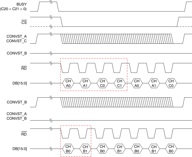
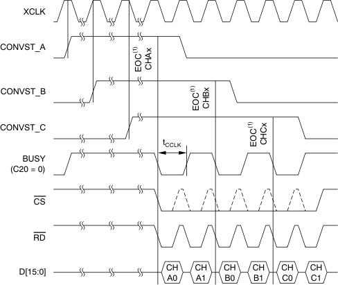
If a parallel interface is used, the behavior of the output port depends on which CONVST_x signals are issued. Figure 30 shows examples of different scenarios.
NOTE:
Boxed areas indicate the minimum required frame to acquire all data.7.3.1.5 BUSY/INT
The BUSY signal indicates if a conversion is in progress. The BUSY signal goes high with a rising edge of any CONVST_x signal and goes low when the output data of the last channel pair are available in the respective output register. The readout of the data can be initiated immediately after the falling edge of BUSY.
In sequential mode, the BUSY signal goes low only for one clock cycle; see the Sequential Mode section for more details.
The INT output goes high at completion of a conversion process and remains high after first read data access.
The polarity of the BUSY/INT signal can be changed using Table 5 bit C20.
7.3.1.6 Reference
The ADS8555 device provides an internal, low-drift, 2.5-V reference source. To increase the input voltage range, the reference voltage can be switched to 3-V mode using the VREF bit (bit C18 in the CR). The reference feeds a 10-bit string-DAC controlled by bits C[9:0] in the control register. The buffered DAC output is connected to the REFIO pin. In this way, the voltage at this pin is programmable in 2.44 mV (2.92 mV in 3-V mode) steps and adjustable to the application needs without additional external components. The actual output voltage can be calculated using Equation 3:

where
- Range = the chosen maximum reference voltage output range (2.5 V or 3 V)
- Code = the decimal value of the DAC register content
Table 1 lists some examples of internal reference DAC settings with a reference range set to 2.5 V. However, to ensure proper performance, the DAC output voltage should not be programmed below 0.5 V.
Decouple the buffered output of the DAC with a 100-nF capacitor (minimum); for best performance, TI recommends a 470-nF capacitor. If the internal reference is placed into power-down (default), an external reference voltage can drive the REFIO pin.
The voltage at the REFIO pin is buffered with three internal amplifiers, one for each ADC pair. The output of each buffer must be decoupled with a 10-μF capacitor between pin pairs 53 and 54, 55 and 56, and 57 and 58. The 10-μF capacitors are available as ceramic 0805-SMD components and in X5R quality.
The internal reference buffers can be powered down to decrease the power dissipation of the device. In this case, external reference drivers can be connected to REFC_A, REFC_B, and REFC_C pins. With 10-μF decoupling capacitors, the minimum required bandwidth can be calculated using Equation 4.

With the minimum tCONV of 1.26 μs, the external reference buffers require a minimum bandwidth of 88 kHz.
Table 1. DAC Setting Examples (2.5-V Operation)
| VREF OUT
(V) |
DECIMAL CODE |
BINARY CODE |
HEXADECIMAL CODE |
|---|---|---|---|
| 0.5 | 204 | 00 1100 1100 | CC |
| 1.25 | 511 | 01 1111 1111 | 1FF |
| 2.5 | 1023 | 11 1111 1111 | 3FF |
7.3.2 Digital
This section describes the digital control and the timing of the device in detail.
7.3.2.1 Device Configuration
Depending on the desired mode of operation, the ADS8555 device can be configured using the external pins or the control register (see Table 5), as shown in Table 2.
Table 2. ADS8555 Configuration Settings
| INTERFACE MODE | HARDWARE MODE (HW/SW = 0) CONVERSION START CONTROLLED BY SEPARATE CONVST_x PINS |
SOFTWARE MODE (HW/SW = 1) CONVERSION START CONTROLLED BY CONVST_A PIN ONLY, EXCEPT IN SEQUENTIAL MODE |
|---|---|---|
| Parallel (PAR/SER = 0) |
Configuration using pins, optionally, control bits C[22:18], C[15:13], and C[9:0] | Configuration using control register bits C[31:0] only; status of pins 27 (only if used as RANGE input) and 63 is disregarded |
| Serial (PAR/SER = 1) |
Configuration using pins, optionally, control bits C[22:18], C[15:13], and C[9:0]; bits C[31:24] are disregarded | Configuration using control register bits C[31:0] only; status of pins 1, 27 (only if used as RANGE input), and 63 is disregarded; each access requires a control register update through SDI (see the Serial Interface section for details) |
7.3.2.2 Parallel Interface
To use the device with the parallel interface, hold the PAR/SER pin low. The maximum achievable data throughput rate using the internal clock is 630 kSPS in this case.
Access to the ADS8555 device is controlled as illustrated in Figure 2 and Figure 3.
The device can either operate with a 16-bit (WORD/BYTE pin set low) or an 8-bit (WORD/BYTE pin set high) parallel interface. If 8-bit operation is used, the HBEN pin selects if the low-byte (DB7 low) or the high-byte (DB7 high) is available on the data output DB[15:8] first.
7.3.2.3 Serial Interface
The serial interface mode is selected by setting the PAR/SER pin high. In this case, each data transfer starts with the falling edge of the frame synchronization input (FS). The conversion results are presented on the serial data output pins SDO_A, SDO_B, and SDO_C depending on the selections made using the SEL_x pins. Starting with the most significant bit (MSB), the output data are changed at the rising edge of SCLK, so that the host processor can read it at the following falling edge.
Serial data input SDI are latched at the falling edge of SCLK.
The serial interface can be used with one, two, or three output ports. These ports are enabled with pins SEL_A, SEL_B, and SEL_C. If all three serial data output ports (SDO_A, SDO_B, and SDO_C) are selected, the data can be read with either two 16-bit data transfers or with one 32-bit data transfer. The data of channels CH_x0 are available first, followed by data from channels CH_x1. The maximum achievable data throughput rate is 450 kSPS in this case.
If the application allows a data transfer using two ports only, SDO_A and SDO_B outputs are used. The device outputs data from channel CH_A0 followed by CH_A1 and CH_C0 on SDO_A, and data from channel CH_B0 followed by CH_B1 and CH_C1 occurs on SDO_B. In this case, a data transfer of three consecutive 16-bit words or one continuous 48-bit word is supported. The maximum achievable data throughput rate is 375 kSPS.
The output SDO_A is selected if only one serial data port is used in the application. The data are available in the following order: CH_A0, CH_A1, CH_B0, CH_B1, CH_C0, and, finally CH_C1. Data can be read using six 16-bit transfers, three 32-bit transfers, or a single 96-bit transfer. The maximum achievable data throughput rate is 250 kSPS in this case.
Figure 1 (the serial operation timing diagram) and Figure 31 illustrate all possible scenarios in more detail.
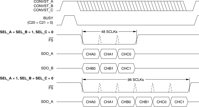 Figure 31. Serial Interface: Data Output With One or Two Active SDOs
7.3.2.4 Output Data Format
The data output format of the ADS8555 is binary twos complement, as shown in Table 3.
Table 3. Output Data Format
| DESCRIPTION | INPUT VOLTAGE VALUE | BINARY CODE (HEXADECIMAL CODE) |
|---|---|---|
| Positive full-scale | 4 VREF or 2 VREF | 0111 1111 1111 1111 (7FFF) |
| Midscale + 0.5 LSB | VREF / (2 × resolution) | 0000 0000 0000 0000 (0000) |
| Midscale – 0.5 LSB | –VREF / (2 × resolution) | 1111 1111 1111 1111 (FFFF) |
| Negative full-scale | –4 VREF or –2 VREF | 1000 0000 0000 0000 (8000) |
7.4 Device Functional Modes
7.4.1 Hardware Mode
With the HW/SW input (pin 62) set low, the device functions are controlled through the pins and, optionally, control register bits C[22:18], C[15:13], and C[9:0].
Generally, the device can be used in hardware mode and switched into software mode to initialize or adjust the control register settings (for example, the internal reference DAC) and then switched back to hardware mode thereafter.
7.4.2 Software Mode
When the HW/SW input is set high, the device operates in software mode with functionality set only by the control register bits (corresponding pin settings are ignored).
If parallel interface is used, an update of all control register settings is performed by issuing two 16-bit write accesses on pins DB[15:0] in word mode or four 8-bit accesses on pins DB[15:8] in byte mode (to avoid losing data, the entire sequence must be finished before starting a new conversion). Hold CS low during the two or four write accesses to completely update the configuration register. Updating only the upper eight bits (C[31:24]) is possible using a single write access and pins DB[15:8] in both word and byte modes. In word mode, the first write access updates only the upper eight bits and stores the lower eight bits (C[23:16]) for an update that takes place with the second write access along with C[15:0].
If the serial interface is used, input data containing control register contents are required with each read access to the device in this mode (combined read/write access). For initialization purposes, all 32 bits of the register must be set (bit C16 must be set to 1 during that access to allow the update of the entire register content). To minimize switching noise on the interface, an update of the first eight bits (C[31:24]) with the remaining bits held low can be performed thereafter.
Figure 35 illustrates the different control register update options.
7.4.3 Daisy-Chain Mode (In Serial Mode Only)
The serial interface of the ADS8555 device supports a daisy-chain feature that allows cascading of multiple devices to minimize the board space requirements and simplify routing of the data and control lines. In this case, pins DB5/DCIN_A, DB4/DCIN_B, and DB3/DCIN_C are used as serial data inputs for channels A, B, and C, respectively. Figure 32 shows an example of a daisy-chain connection of three devices sharing a common CONVST line to allow simultaneous sampling of 18 analog channels along with the corresponding timing diagram. To activate the daisy-chain mode, the DCEN pin must be pulled high. As a result of the time specifications tS1, tH1, and tD3, the maximum SCLK frequency that may be used in daisy-chain mode is 27.78 MHz (assuming 50% duty cycle).
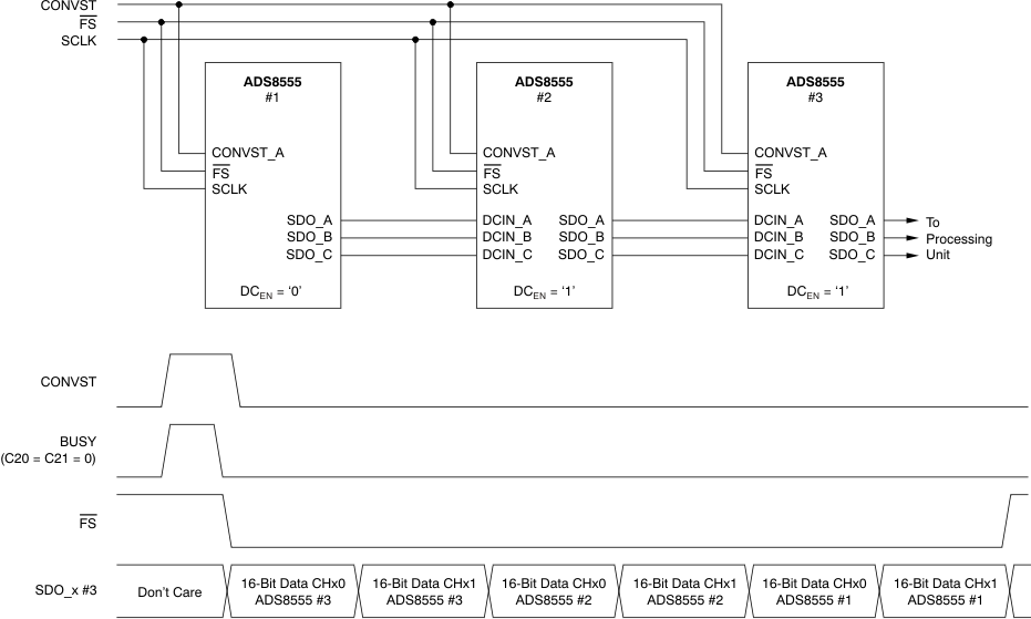 Figure 32. Example of Daisy-Chaining Three ADS8555 Devices
7.4.4 Sequential Mode (In Software Mode With External Conversion Clock Only)
The three channel pairs of the ADS8555 device can be run in sequential mode, with the corresponding CONVST_x signals interleaved, when an external clock is used. To activate the device in sequential mode, CR bits C11 (CLKSEL) and C23 (SEQ) must be asserted. In this case, the BUSY output indicates a finished conversion by going low (when C20 = 0) or high (when C20 = 1) for only a single conversion clock cycle in case of ongoing conversions of any other channel pairs. Figure 33 shows the behavior of the BUSY output in this mode. Initiate each conversion start during the high phase of the external clock, as shown in Figure 33. The minimum time required between two CONVST_x pulses is the time required to read the conversion result of a channel (pair).
7.4.5 Reset and Power-Down Modes
The device supports two reset mechanisms: a power-on reset (POR) and a pin-controlled reset (RESET) that can be issued using pin 28. Both the POR and RESET act as a master reset that causes any ongoing conversion to be interrupted, the control register content to be set to the default value, and all channels to be switched into sample mode.
When the device is powered up, the POR sets the device in default mode when AVDD reaches 1.5 V. When the device is powered down, the POR circuit requires AVDD to remain below 125 mV at least 350 ms to ensure proper discharging of internal capacitors and to ensure correct behavior of the device when powered up again. If the AVDD drops below 400 mV but remains above 125 mV (see the undefined zone in Figure 34), the internal POR capacitor does not discharge fully and the device requires a pin-controlled reset to perform correctly after the recovery of AVDD.
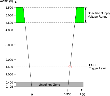 Figure 34. POR: Relevant Voltage Levels
The entire device, except the digital interface, can be powered down by pulling the STBY pin low (pin 24). Because the digital interface section remains active, data can be retrieved when in stand-by mode. To power the device on again, the STBY pin must be brought high. The device is ready to start a new conversion after the 10 ms required to activate and settle the internal circuitry. This user-controlled approach can be used in applications that require lower data throughput rates and lowest power dissipation. The content of CR is not changed during standby mode. A pin-controlled reset is not required after returning to normal operation.
Although the standby mode affects the entire device, each device channel pair can also be individually switched off by setting control register bits C[15:13] (PD_x). When reactivated, the relevant channel pair requires 10 ms to fully settle before starting a new conversion. The internal reference remains active, except all channels are powered down at the same time.
The auto-NAP power-down mode is enabled by asserting the A-NAP bit (C22) in the control register. If the auto-NAP mode is enabled, the ADS8555 device automatically reduces the current requirement to 6 mA after finishing a conversion; thus, the end of conversion actually activates the power-down mode. Triggering a new conversion by applying a positive CONVST_x edge puts the device back into normal operation, starts the acquisition of the analog input, and automatically starts a new conversion six conversion clock cycles later. Therefore, a complete conversion cycle takes 24.5 conversion clock cycles; thus, the maximum throughput rate in auto-NAP power-down mode is reduced to a maximum of 380 kSPS in serial mode, and 500 kSPS in parallel mode. The internal reference remains active during the auto-NAP mode. Table 4 compares the analog current requirements of the device in the different modes.
Table 4. Maximum Analog Current (IAVDD) Demand of the ADS8555
7.5 Register Maps
7.5.1 Control Register (CR); Default Value = 0x000003FF
The control register settings can only be changed in software mode and are not affected when switching to hardware mode thereafter. The register values are independent from input pin settings. Changes are active with the rising edge of WR in parallel interface mode or with the 32nd falling SCLK edge of the access in which the register content has been updated in serial mode. Optionally, the register can also be partially updated by writing only the upper eight bits (C[31:24]). The CR content is defined in Table 5.
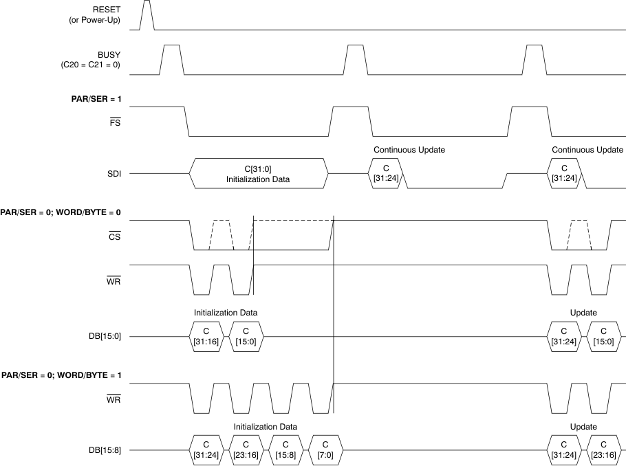 Figure 35. Control Register Update Options