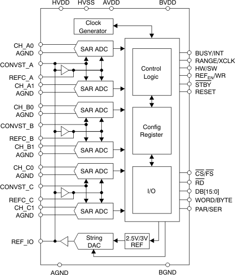
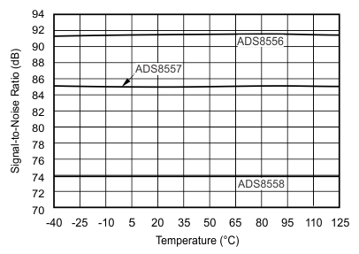
The ADS855x contains six low-power, 16-, 14-, or 12-bit, successive approximation register (SAR) based analog-to-digital converters (ADCs) with true bipolar inputs. Each channel contains a sample-and-hold circuit that allows simultaneous high-speed multi-channel signal acquisition.
The ADS855x supports data rates of up to 730 kSPS in parallel interface mode or up to 500 kSPS if the serial interface is used. The bus width of the parallel interface can be set to eight or 16 bits. In serial mode, up to three output channels can be activated.
The ADS855x is specified over the full industrial temperature range of –40°C to 125°C and is available in an LQFP-64 package.
PART NUMBER | PACKAGE | BODY SIZE (NOM) |
---|---|---|
ADS8556 | LQFP (64) | 10.00 mm × 10.00 mm |
ADS8557 | ||
ADS8558 |
Changes from C Revision (November 2015) to D Revision
Changes from B Revision (January 2012) to C Revision
Changes from A Revision (August 2009) to B Revision
PIN | TYPE(1) | DESCRIPTION | ||
---|---|---|---|---|
NAME | NO. | PARALLEL INTERFACE (PAR/SER = 0) | SERIAL INTERFACE (PAR/SER = 1) | |
DB14/REFBUFEN | 1 | DIO, DI | Data bit 14 input/output Output is '0' for the ADS8557, ADS8558 |
Hardware mode (HW/SW = 0): Reference buffers enable input. When low, all reference buffers are enabled (mandatory if internal reference is used). When high, all reference buffers are disabled. |
Software mode (HW/SW = 1): Connect to BGND or BVDD. The reference buffers are controlled by bit C24 (REFBUF) in control register (CR). |
||||
DB13/SDI | 2 | DIO, DI | Data bit 13 input/output Output is MSB for the ADS8557 and '0' for the ADS8558 |
Hardware mode (HW/SW = 0): Connect to BGND |
Software mode (HW/SW = 1): Serial data input |
||||
DB12 | 3 | DIO | Data bit 12 input/output Output is '0' for the ADS8558 |
Connect to BGND |
DB11 | 4 | DIO | Data bit 11 input/output Output is MSB for the ADS8558 |
Connect to BGND |
DB10/SDO_C | 5 | DIO, DO | Data bit 10 input/output | When SEL_C = 1, data output for channel C When SEL_C = 0, tie this pin to BGND |
DB9/SDO_B | 6 | DIO, DO | Data bit 9 input/output | When SEL_B = 1, data output for channel B When SEL_B = 0, tie this pin to BGND When SEL_C = 0, data from channel C1 are also available on this output |
DB8/SDO_A | 7 | DIO, DO | Data bit 8 input/output | Data output for channel A When SEL_C = 0, data from channel C0 are also available on this output When SEL_C = 0 and SEL_B = 0, SDO_A acts as the single data output for all channels |
BGND | 8 | P | Buffer IO ground, connect to digital ground plane | |
BVDD | 9 | P | Buffer IO supply, connect to digital supply (2.7 V to 5.5 V). Decouple with a 1-μF ceramic capacitor or a combination of 100-nF and 10-μF ceramic capacitors to BGND. | |
DB7/HBEN/DCEN | 10 | DIO, DI, DI | Word mode (WORD/BYTE = 0): Data bit 7 input/output | Daisy-chain enable input. When high, DB[5:3] serve as daisy-chain inputs DCIN[A:C]. If daisy-chain mode is not used, connect to BGND. |
Byte mode (WORD/BYTE = 1): High byte enable input. When high, the high byte is output first on DB[15:8]. When low, the low byte is output first on DB[15:8]. |
||||
DB6/SCLK | 11 | DIO, DI | Word mode (WORD/BYTE = 0): Data bit 6 input/output |
Serial interface clock input (36 MHz, max) |
Byte mode (WORD/BYTE = 1): Connect to BGND or BVDD |
||||
DB5/DCIN_A | 12 | DIO, DI | Word mode (WORD/BYTE = 0): Data bit 5 input/output |
When DCEN = 1, daisy-chain data input for channel A. When DCEN = 0, connect to BGND. |
Byte mode (WORD/BYTE = 1): Connect to BGND or BVDD |
||||
DB4/DCIN_B | 13 | DIO, DI | Word mode (WORD/BYTE = 0): Data bit 4 input/output |
When SEL_B = 1 and DCEN = 1, daisy-chain data input for channel B. When DCEN = 0, connect to BGND. |
Byte mode (WORD/BYTE = 1): Connect to BGND or BVDD |
||||
DB3/DCIN_C | 14 | DIO, DI | Word mode (WORD/BYTE = 0): Data bit 3 input/output |
When SEL_C = 1 and DCEN = 1, daisy-chain data input for channel C. When DCEN = 0, connect to BGND. |
Byte mode (WORD/BYTE = 1): Connect to BGND or BVDD |
||||
DB2/SEL_C | 15 | DIO, DI | Word mode (WORD/BYTE = 0): Data bit 2 input/output |
Select SDO_C input. When high, SDO_C is active. When low, SDO_C is disabled. |
Byte mode (WORD/BYTE = 1): Connect to BGND or BVDD |
||||
DB1/SEL_B | 16 | DIO, DI | Word mode (WORD/BYTE = 0): Data bit 1 input/output |
Select SDO_B input. When high, SDO_B is active. When low, SDO_B is disabled. |
Byte mode (WORD/BYTE = 1): Connect to BGND or BVDD |
||||
DB0/SEL_A | 17 | DIO, DI | Word mode (WORD/BYTE = 0): Data bit 0 (LSB) input/output |
Select SDO_A input. When high, SDO_A is active. When low, SDO_A is disabled. Must always be high. |
Byte mode (WORD/BYTE = 1): Connect to BGND or BVDD |
||||
BUSY/INT | 18 | DO | When CR bit C21 = 0 (BUSY/INT), converter busy status output. Transitions high when a conversion has been started and remains high during the entire process. Transitions low when the conversion data of all six channels are latched to the output register and remains low thereafter. In sequential mode (SEQ = 1 in the CR), the BUSY output transitions high when a conversion has been started and goes low for a single conversion clock cycle (tCCLK) whenever a channel pair conversion is completed. When bit C21 = 1 (BUSY/INT in CR), interrupt output. This bit transitions high after a conversion completes and remains high until the conversion result is read. The polarity of BUSY/INT output can be changed using bit C20 (BUSY L/H) in the control register. |
|
CS/FS | 19 | DI, DI | Chip select input. When low, the parallel interface is enabled. When high, the interface is disabled. |
Frame synchronization. The falling edge of FS controls the frame transfer. |
RD | 20 | DI | Read data input. When low, the parallel data output is enabled. When high, the data output is disabled. |
Connect to BGND. |
CONVST_C | 21 | DI | Hardware mode (HW/SW = 0): Conversion start of channel pair C. The rising edge of this signal initiates simultaneous conversion of analog signals at inputs CH_C[1:0]. CONVST_C must remain high during the entire conversion cycle, otherwise both ADCs of channel C are put in partial power-down mode (see the Reset and Power-Down Modes section). |
|
Software mode (HW/SW = 1): Conversion start of channel pair C in sequential mode (CR bit C23 = 1) only; connect to BGND or BVDD otherwise. | ||||
CONVST_B | 22 | DI | Hardware mode (HW/SW = 0): Conversion start of channel pair B. The rising edge of this signal initiates simultaneous conversion of analog signals at inputs CH_B[1:0]. CONVST_B must remain high during the entire conversion cycle; otherwise, both ADCs of channel B are put into partial power-down mode (see the Reset and Power-Down Modes section). |
|
Software mode (HW/SW = 1): Conversion start of channel pair B in sequential mode (CR bit C23 = 1) only; connect to BGND or BVDD otherwise. | ||||
CONVST_A | 23 | DI | Hardware mode (HW/SW = 0): Conversion start of channel pair A. The rising edge of this signal initiates simultaneous conversion of analog signals at inputs CH_A[1:0]. CONVST_A must remain high during the entire conversion cycle; otherwise, both ADCs of channel A are put into partial power-down mode (see the Reset and Power-Down Modes section). |
|
Software mode (HW/SW = 1): Conversion start of all selected channels except in sequential mode (CR bit C23 = 1): Conversion start of channel pair A only. |
||||
STBY | 24 | DI | Standby mode input. When low, the entire device is powered-down (including the internal clock and reference). When high, the device operates in normal mode. |
|
AGND | 25, 32, 37, 38, 43, 44, 49, 52, 53, 55, 57, 59 | P | Analog ground, connect to analog ground plane Pin 25 can have a dedicated ground if the difference between its potential and AGND is always kept within ±300 mV. |
|
AVDD | 26, 34, 35, 40, 41, 46, 47, 50, 60 | P | Analog power supply (4.5 V to 5.5 V). Decouple each pin with a 100-nF ceramic capacitor to AGND. Use an additional 10-μF capacitor to AGND close to the device but without compromising the placement of the smaller capacitor. Pin 26 can have a dedicated power supply if the difference between its potential and AVDD is always kept within ±300 mV. | |
RANGE/XCLK | 27 | DI, DIO | Hardware mode (HW/SW = 0): Input voltage range select input. When low, the analog input range is ±4 VREF. When high, the analog input range is ±2 VREF. |
|
Software mode (HW/SW = 1): External conversion clock input, if CR bit C11 (CLKSEL) is set high or internal conversion clock output, if CR bit C10 (CLKOUT_EN) is set high. If not used, connect to BVDD or BGND. | ||||
RESET | 28 | DI | Reset input, active high. Aborts any ongoing conversions. Resets the internal control register to 0x000003FF. The RESET pulse must be at least 50 ns long. | |
WORD/BYTE | 29 | DI | Output mode selection input. When low, data are transferred in word mode using DB[15:0]. When high, data are transferred in byte mode using DB[15:8] with the byte order controlled by HBEN pin while two accesses are required for a complete 16-bit transfer. |
Connect to BGND. |
HVSS | 30 | P | Negative supply voltage for the analog inputs (–16.5 V to –5 V). Decouple with a 100-nF ceramic capacitor to AGND placed next to the device and a 10-μF capacitor to AGND close to the device but without compromising the placement of the smaller capacitor. |
|
HVDD | 31 | P | Positive supply voltage for the analog inputs (5 V to 16.5 V). Decouple with a 100-nF ceramic capacitor to AGND placed next to the device and a 10-μF capacitor to AGND close to the device but without compromising the placement of the smaller capacitor. | |
CH_A0 | 33 | AI | Analog input of channel A0. The input voltage range is controlled by RANGE pin in hardware mode or CR bit C26 (RANGE_A) in software mode. | |
CH_A1 | 36 | AI | Analog input of channel A1. The input voltage range is controlled by RANGE pin in hardware mode or CR bit C26 (RANGE_A) in software mode. | |
CH_B0 | 39 | AI | Analog input of channel B0. The input voltage range is controlled by RANGE pin in hardware mode or CR bit C27 (RANGE_B) in software mode. | |
CH_B1 | 42 | AI | Analog input of channel B1. The input voltage range is controlled by RANGE pin in hardware mode or CR bit C27 (RANGE_B) in software mode. | |
CH_C0 | 45 | AI | Analog input of channel C0. The input voltage range is controlled by RANGE pin in hardware mode or CR bit C28 (RANGE_C) in software mode. | |
CH_C1 | 48 | AI | Analog input of channel C1. The input voltage range is controlled by RANGE pin in hardware mode or CR bit C28 (RANGE_C) in software mode. | |
REFIO | 51 | AIO | Reference voltage input/output (0.5 V to 3.025 V). The internal reference is enabled via REFEN/WR pin in hardware mode or CR bit C25 (REFEN) in software mode. The output value is controlled by the internal DAC (CR bits C[9:0]). Connect a 470-nF ceramic decoupling capacitor between this pin and pin 52. |
|
REFC_A | 54 | AI | Decoupling capacitor for reference of channels A. Connect a 10-μF ceramic decoupling capacitor between this pin and pin 53. |
|
REFC_B | 56 | AI | Decoupling capacitor for reference of channels B. Connect a 10-μF ceramic decoupling capacitor between this pin and pin 55. |
|
REFC_C | 58 | AI | Decoupling capacitor for reference of channels C. Connect a 10-μF ceramic decoupling capacitor between this pin and pin 57. |
|
PAR/SER | 61 | DI | Interface mode selection input. When low, the parallel interface is selected. When high, the serial interface is enabled. |
|
HW/SW | 62 | DI | Mode selection input. When low, the hardware mode is selected and part works according to the settings of external pins. When high, the software mode is selected in which the device is configured by writing into the control register. |
|
REFEN/WR | 63 | DI | Hardware mode (HW/SW = 0): Internal reference enable input. When high, the internal reference is enabled (the reference buffers are to be enabled). When low, the internal reference is disabled and an external reference is applied at REFIO. |
Hardware mode (HW/SW = 0): Internal reference enable input. When high, the internal reference is enabled (the reference buffers are to be enabled). When low, the internal reference is disabled and an external reference must be applied at REFIO. |
Software mode (HW/SW = 1): Write input. The parallel data input is enabled, when CS and WR are low. The internal reference is enabled by the CR bit C25 (REFEN). |
Software mode (HW/SW = 1): Connect to BGND or BVDD. The internal reference is enabled by CR bit C25 (REFEN). |
|||
DB15 | 64 | DIO | Data bit 15 (MSB) input/output. Output is '0' for the ADS8557/8. |
Connect to BGND. |
MIN | MAX | UNIT | |
---|---|---|---|
Supply voltage, HVDD to AGND | –0.3 | 18 | V |
Supply voltage, HVSS to AGND | –18 | 0.3 | V |
Supply voltage, AVDD to AGND | –0.3 | 6 | V |
Supply voltage, BVDD to BGND | –0.3 | 6 | V |
Analog input voltage | HVSS – 0.3 | HVDD + 0.3 | V |
Reference input voltage with respect to AGND | AGND – 0.3 | AVDD + 0.3 | V |
Digital input voltage with respect to BGND | BGND – 0.3 | BVDD + 0.3 | V |
Ground voltage difference AGND to BGND | ±0.3 | V | |
Input current to all pins except supply | –10 | 10 | mA |
Maximum virtual junction temperature, TJ | 150 | °C | |
Storage Temperature, Tstg | -65 | 150 | °C |
VALUE | UNIT | |||
---|---|---|---|---|
V(ESD) | Electrostatic discharge | Human-body model (HBM), per ANSI/ESDA/JEDEC JS-001 JEDEC standard 22, test method A114-C.01(1) |
±2000 | V |
Charged-device model (CDM), per JEDEC specification JESD22-C101 JEDEC standard 22, test method C101(2) |
±500 |
MIN | NOM | MAX | UNIT | ||
---|---|---|---|---|---|
Supply voltage, AVDD to AGND | 4.5 | 5 | 5.5 | V | |
Supply voltage, BVDD to BGND | Low-voltage levels | 2.7 | 3.0 | 3.6 | V |
5-V logic levels | 4.5 | 5 | 5.5 | ||
Input supply voltage, HVDD to AGND | Range 1 (±2 × VREF) | 2 × VREF | 16.5 | V | |
Range 2 (±4 × VREF) | 4 × VREF | 16.5 | |||
Input supply voltage, HVSS to AGND | Range 1 (±2 × VREF) | –16.5 | –2 × VREF | V | |
Range 2 (±4 × VREF) | –16.5 | –4 × VREF | |||
Reference input voltage (VREF) | 0.5 | 2.5 | 3.0 | V | |
Analog inputs(1) | Range 1 (±2 × VREF) | –2 × VREF | 2 × VREF | V | |
Range 1 (±4 × VREF) | –4 × VREF | 4 × VREF | |||
Operating ambient temperature, TA | –40 | 125 | °C |
THERMAL METRIC(1) | ADS855x | UNIT | ||
---|---|---|---|---|
PM (LQFP) | ||||
64 PINS | ||||
RθJA | Junction-to-ambient thermal resistance | High-K thermal resistance(2) | 50.3 | °C/W |
RθJC(top) | Junction-to-case (top) thermal resistance | 12.0 | °C/W | |
RθJB | Junction-to-board thermal resistance | 24.0 | °C/W | |
ψJT | Junction-to-top characterization parameter | 0.5 | °C/W | |
ψJB | Junction-to-board characterization parameter | 23.5 | °C/W | |
RθJC(bot) | Junction-to-case (bottom) thermal resistance | NA | °C/W |
PARAMETER | TEST CONDITIONS | MIN | TYP(1) | MAX | UNIT | |
---|---|---|---|---|---|---|
ANALOG INPUT | ||||||
CHXX | Bipolar full-scale range | RANGE pin/RANGE bit = 0 | –4 × VREF | 4 × VREF | V | |
RANGE pin/RANGE bit = 1 | –2 × VREF | 2 × VREF | ||||
Input capacitance | Input range = ±4 × VREF | 10 | pF | |||
Input range = ±2 × VREF | 20 | |||||
Input leakage current | No ongoing conversion | ±1 | μA | |||
Aperture delay | 5 | ns | ||||
Aperture delay matching | Common CONVST for all channels | 250 | ps | |||
Aperture jitter | 50 | ps | ||||
EXTERNAL CLOCK INPUT (XCLK) | ||||||
fXCLK | External clock frequency | An external reference must be used for fXCLK > fCCLK | 1 | 18 | 20 | MHz |
External clock duty cycle | 45% | 55% | ||||
REFERENCE VOLTAGE OUTPUT (REFOUT) | ||||||
VREF | Reference voltage | 2.5-V operation, REFDAC = 0x3FF | 2.485 | 2.5 | 2.515 | V |
2.5-V operation, REFDAC = 0x3FF at 25°C | 2.496 | 2.5 | 2.504 | |||
3-V operation, REFDAC = 0x3FF | 2.985 | 3.0 | 3.015 | |||
3-V operation, REFDAC = 0x3FF at 25°C | 2.995 | 3.0 | 3.005 | |||
dVREF/dT | Reference voltage drift | ±10 | ppm/°C | |||
PSRR | Power-supply rejection ratio | 73 | dB | |||
IREFOUT | Output current | With dc current | –2 | 2 | mA | |
IREFSC | Short-circuit current(2) | 50 | mA | |||
tREFON | Turn-on settling time | 10 | ms | |||
External load capacitance | At CREF_x pins | 4.7 | 10 | μF | ||
At REFIO pins | 100 | 470 | ||||
REFDAC | Tuning range | Internal reference output voltage range | 0.2 × VREF | VREF | V | |
REFDAC resolution | 10 | Bits | ||||
DNLDAC | REFDAC differential nonlinearity | –1 | ±0.1 | 1 | LSB | |
INLDAC | REFDAC integral nonlinearity | –2 | ±0.1 | 2 | LSB | |
VOSDAC | REFDAC offset error | VREF = 0.5 V (DAC = 0x0CC) | –4 | ±0.65 | 4 | LSB |
REFERENCE VOLTAGE INPUT (REFIN) | ||||||
VREFIN | Reference input voltage | 0.5 | 2.5 | 3.025 | V | |
Input resistance | 100 | MΩ | ||||
Input capacitance | 5 | pF | ||||
Reference input current | 1 | μA | ||||
SERIAL CLOCK INPUT (SCLK) | ||||||
fSCLK | Serial clock input frequency | 0.1 | 36 | MHz | ||
tSCLK | Serial clock period | 0.0278 | 10 | μs | ||
Serial clock duty cycle | 40% | 60% | ||||
DIGITAL INPUTS(3) | ||||||
Logic family | CMOS with Schmitt-Trigger | |||||
High-level input voltage | 0.7 × BVDD | BVDD + 0.3 | V | |||
Low-level input voltage | BGND – 0.3 | 0.3 × BVDD | V | |||
Input current | VI = BVDD to BGND | –50 | 50 | nA | ||
Input capacitance | 5 | pF | ||||
DIGITAL OUTPUTS(3) | ||||||
Logic family | CMOS | |||||
High-level output voltage | IOH = 100 μA | BVDD – 0.6 | BVDD | V | ||
Low-level output voltage | IOH = –100 μA | BGND | BGND + 0.4 | V | ||
High-impedance-state output current | –50 | 50 | nA | |||
Output capacitance | 5 | pF | ||||
Load capacitance | 30 | pF | ||||
POWER-SUPPLY REQUIREMENTS | ||||||
AVDD | Analog supply voltage | 4.5 | 5 | 5.5 | V | |
BVDD | Buffer I/O supply voltage | 2.7 | 3 | 5.5 | V | |
HVDD | Input positive supply voltage | 5 | 10 | 16.5 | V | |
HVSS | Input negative supply voltage | –16.5 | –10 | –5 | V | |
IAVDD | Analog supply current(4) | fDATA = maximum | 30 | 36 | mA | |
ADS8556, fDATA = 250 kSPS (auto-NAP mode) | 14 | 16.5 | ||||
ADS8557, fDATA = 250 kSPS (auto-NAP mode) | 14 | 17 | ||||
ADS8558, fDATA = 250 kSPS (auto-NAP mode) | 14 | 18 | ||||
Auto-NAP mode, no ongoing conversion, internal conversion clock | 4 | 6 | ||||
Power-down mode | 0.1 | 50 | μA | |||
IBVDD | Buffer I/O supply current(5) | fDATA = maximum | 0.9 | 2 | mA | |
fDATA = 250 kSPS (auto-NAP mode) | 0.5 | 1.5 | ||||
Auto-NAP mode, no ongoing conversion, internal conversion clock | 0.1 | 10 | μA | |||
Power-down mode | 0.1 | 10 | ||||
IHVDD | Input positive supply current(6) | ADS8556, fDATA = maximum | 3 | 3.5 | mA | |
ADS8557, fDATA = maximum | 3.1 | 3.6 | ||||
ADS8558, fDATA = maximum | 3.3 | 4 | ||||
fDATA = 250 kSPS (auto-NAP mode) | 1.6 | 2 | ||||
Auto-NAP mode, no ongoing conversion, internal conversion clock | 0.2 | 0.3 | μA | |||
Power-down mode | 0.1 | 10 | ||||
IHVSS | Input negative supply current(7) | ADS8556, fDATA = maximum | 3.6 | 4 | mA | |
ADS8557, fDATA = maximum | 3.6 | 4.2 | ||||
ADS8558, fDATA = maximum | 4 | 4.8 | ||||
fDATA = 250 kSPS (auto-NAP mode) | 1.8 | 2.2 | ||||
Auto-NAP mode, no ongoing conversion, internal conversion clock | 0.2 | 0.25 | μA | |||
Power-down mode | 0.1 | 10 | ||||
Power dissipation(8) | ADS8556, fDATA = maximum | 251.7 | 298.5 | mW | ||
ADS8557, fDATA = maximum | 253.2 | 303 | ||||
ADS8558, fDATA = maximum | 262.2 | 318 | ||||
ADS8556, fDATA = 250 kSPS (auto-NAP mode) | 122.5 | 150 | ||||
ADS8557, fDATA = 250 kSPS (auto-NAP mode) | 122.5 | 152.5 | ||||
ADS8558, fDATA = 250 kSPS (auto-NAP mode) | 122.5 | 157.5 | ||||
Auto-NAP mode, no ongoing conversion, internal conversion clock | 26 | 38.3 | ||||
Power-down mode | 3.8 | 580 | μW |
PARAMETER | TEST CONDITIONS | MIN | TYP(1) | MAX | UNIT | |
---|---|---|---|---|---|---|
DC ACCURACY | ||||||
Resolution | 16 | Bits | ||||
No missing codes | 16 | Bits | ||||
INL | Integral linearity error | At TA = –40°C to 85°C | –3 | ±1.5 | 3 | LSB |
At TA = –40°C to 125°C | –4 | ±1.5 | 4 | |||
DNL | Differential linearity error | At TA = –40°C to 85°C | –1 | ±0.75 | 1.5 | LSB |
At TA = –40°C to 125°C | –1 | ±0.75 | 2 | |||
Offset error | –4 | ±0.8 | 4 | mV | ||
Offset error drift | ±3.5 | μV/°C | ||||
Gain error | Referenced to voltage at REFIO | –0.75 | ±0.25 | 0.75 | %FSR | |
Gain error drift | Referenced to voltage at REFIO | ±6 | ppm/°C | |||
PSRR | Power-supply rejection ratio | At output code FFFFh, related to AVDD | 60 | dB | ||
SAMPLING DYNAMICS | ||||||
tACQ | Acquisition time | 280 | ns | |||
tCONV | Conversion time per ADC | 1.26 | μs | |||
tCCLK | Internal conversion clock period | 18.5 | tCCLK | |||
68.0 | ns | |||||
fDATA | Throughput rate | Parallel interface, internal clock and reference | 630 | kSPS | ||
Serial interface, internal clock and reference | 450 | |||||
AC ACCURACY | ||||||
SNR | Signal-to-noise ratio | At fIN = 10 kHz, TA = –40°C to 85°C | 90 | 91.5 | dB | |
At fIN = 10 kHz, TA = –40°C to 125°C | 89 | 91.5 | ||||
SINAD | Signal-to-noise ratio + distortion | At fIN = 10 kHz, TA = –40°C to 85°C | 87 | 89.5 | dB | |
At fIN = 10 kHz, TA = –40°C to 125°C | 86.5 | 89.5 | ||||
THD | Total harmonic distortion(2) | At fIN = 10 kHz, TA = –40°C to 85°C | –94 | –90 | dB | |
At fIN = 10 kHz, TA = –40°C to 125°C | –94 | –89.5 | ||||
SFDR | Spurious-free dynamic range | At fIN = 10 kHz, TA = –40°C to 85°C | 90 | 95 | dB | |
At fIN = 10 kHz, TA = –40°C to 125°C | 89.5 | 95 | ||||
Channel-to-channel isolation | At fIN = 10 kHz | 100 | dB | |||
–3-dB small-signal bandwidth | In 4 × VREF mode | 48 | MHz | |||
In 2 × VREF mode | 24 |
PARAMETER | TEST CONDITIONS | MIN | TYP(1) | MAX | UNIT | |
---|---|---|---|---|---|---|
DC ACCURACY | ||||||
Resolution | 14 | Bits | ||||
No missing codes | 14 | Bits | ||||
INL | Integral linearity error | –1 | ±0.4 | 1 | LSB | |
DNL | Differential linearity error | –1 | ±0.25 | 1 | LSB | |
Offset error | –4 | ±0.8 | 4 | mV | ||
Offset error drift | ±3.5 | μV/°C | ||||
Gain error | Referenced to voltage at REFIO | –0.75 | ±0.25 | 0.75 | %FSR | |
Gain error drift | Referenced to voltage at REFIO | ±6 | ppm/°C | |||
PSRR | Power-supply rejection ratio | At output code FFFFh, related to AVDD | 60 | dB | ||
SAMPLING DYNAMICS | ||||||
tACQ | Acquisition time | 280 | ns | |||
tCONV | Conversion time per ADC | 1.19 | μs | |||
tCCLK | Internal conversion clock period | 18.5 | tCCLK | |||
64.1 | ns | |||||
fDATA | Throughput rate | Parallel interface, internal clock and reference | 670 | kSPS | ||
Serial interface, internal clock and reference | 470 | |||||
AC ACCURACY | ||||||
SNR | Signal-to-noise ratio | At fIN = 10 kHz | 84 | 85 | dB | |
SINAD | Signal-to-noise ratio + distortion | At fIN = 10 kHz | 83 | 84 | dB | |
THD | Total harmonic distortion(2) | At fIN = 10 kHz | –91 | –86 | dB | |
SFDR | Spurious-free dynamic range | At fIN = 10 kHz | 86 | 92 | dB | |
Channel-to-channel isolation | At fIN = 10 kHz | 100 | dB | |||
–3-dB small-signal bandwidth | In 4 × VREF mode | 48 | MHz | |||
In 2 × VREF mode | 24 |
PARAMETER | TEST CONDITIONS | MIN | TYP(1) | MAX | UNIT | |
---|---|---|---|---|---|---|
DC ACCURACY | ||||||
Resolution | 12 | Bits | ||||
No missing codes | 12 | Bits | ||||
INL | Integral linearity error | –0.75 | ±0.2 | 0.75 | LSB | |
DNL | Differential linearity error | –0.5 | ±0.2 | 0.5 | LSB | |
Offset error | –4 | ±0.8 | 4 | mV | ||
Offset error drift | ±3.5 | μV/°C | ||||
Gain error | Referenced to voltage at REFIO | –0.75 | ±0.25 | 0.75 | %FSR | |
Gain error drift | Referenced to voltage at REFIO | ±6 | ppm/°C | |||
PSRR | Power-supply rejection ratio | At output code FFFFh, related to AVDD | 60 | dB | ||
SAMPLING DYNAMICS | ||||||
tACQ | Acquisition time | 280 | ns | |||
tCONV | Conversion time per ADC | 1.09 | μs | |||
tCCLK | Internal conversion clock period | 18.5 | tCCLK | |||
58.8 | ns | |||||
fDATA | Throughput rate | Parallel interface, internal clock and reference | 730 | kSPS | ||
Serial interface, internal clock and reference | 500 | |||||
AC ACCURACY | ||||||
SNR | Signal-to-noise ratio | At fIN = 10kHz | 73 | 73.9 | dB | |
SINAD | Signal-to-noise ratio + distortion | At fIN = 10kHz | 73 | 73.8 | dB | |
THD | Total harmonic distortion(2) | At fIN = 10kHz | –89 | –84 | dB | |
SFDR | Spurious-free dynamic range | At fIN = 10kHz | 84 | 92 | dB | |
Channel-to-channel isolation | At fIN = 10kHz | 100 | dB | |||
–3-dB small-signal bandwidth | In 4 × VREF mode | 48 | MHz | |||
In 2 × VREF mode | 24 |
MIN | NOM | MAX | UNIT | |||
---|---|---|---|---|---|---|
tACQ | Acquisition time | 280 | ns | |||
tCONV | Conversion time | ADS8556 | 1.26 | µs | ||
ADS8557 | 1.19 | |||||
ADS8558 | 1.09 | |||||
t1 | CONVST_x low time | 20 | ns | |||
t2 | BUSY low to CS low time | 0 | ns | |||
t3 | Bus access finished to next conversion start time(2) | ADS8556 | 40 | ns | ||
ADS8557 | 20 | |||||
ADS8558 | 0 | |||||
t4 | CS low to RD low time | 0 | ns | |||
t5 | RD high to CS high time | 0 | ns | |||
t6 | RD pulse duration | 30 | ns | |||
t7 | Minimum time between two read accesses | 10 | ns | |||
tD1 | CONVST_x high to BUSY high delay | 5 | 20 | ns | ||
tD5 | RD falling edge to output data valid delay | 20 | ns | |||
tH3 | Output data to RD rising edge hold time | 5 | ns |
MIN | NOM | MAX | UNIT | ||
---|---|---|---|---|---|
t8 | CS low to WR low time | 0 | ns | ||
t9 | WR low pulse duration | 15 | ns | ||
t10 | WR high pulse duration | 10 | ns | ||
t11 | WR high to CS high time | 0 | ns | ||
tS2 | Output data to WR rising edge setup time | 5 | ns | ||
tH4 | Data output to WR rising edge hold time | 5 | ns |
AVDD = BVDD = 5 V | HVSS = –15 V | HVDD = 15 V |
fDATA = max | Internal reference |
AVDD = BVDD = 5 V | HVSS = –15 V | HVDD = 15 V |
fDATA = max | Internal reference |
AVDD = BVDD = 5 V | HVSS = –15 V | HVDD = 15 V |
fDATA = max | Internal reference |
AVDD = BVDD = 5 V | HVSS = –15 V | HVDD = 15 V |
fDATA = max | Internal reference |
AVDD = BVDD = 5 V | HVSS = –15 V | HVDD = 15 V |
fDATA = max | Internal reference |
CSUPPLY = 100 nF on AVDD |
AVDD = BVDD = 5 V | HVSS = –15 V | HVDD = 15 V |
Range = 4 × VREF | 8192 samples | Internal reference |
AVDD = BVDD = 5 V | HVSS = –15 V | HVDD = 15 V |
Range = ±4 × VREF | fSIGNAL = 10 kHz | fDATA = max |
Internal reference |
AVDD = BVDD = 5 V | HVSS = –15 V | HVDD = 15 V |
Range = ±4 × VREF | fSIGNAL = 10 kHz | fDATA = max |
Internal reference |
AVDD = BVDD = 5 V | fSAMPLE = 500 kSPS | HVSS = –15 V |
Range = ±2 × VREF | fSIGNAL = 10 kHz | HVDD = 15 V |
Internal reference |
AVDD = 5 V | Internal reference |
Range = ±4 × VREF | HVSS = –15 V | HVDD = 15 V |
Internal reference |
Range = ±4 × VREF | HVSS = –15 V | HVDD = 15 V |
AVDD = BVDD = 5 V | HVSS = –15 V | HVDD = 15 V |
fDATA = max | Internal reference |
AVDD = BVDD = 5 V | HVSS = –15 V | HVDD = 15 V |
fDATA = max | Internal reference |
AVDD = BVDD = 5 V | HVSS = –15 V | HVDD = 15 V |
fDATA = max | Internal reference |
AVDD = BVDD = 5 V | HVSS = –15 V | HVDD = 15 V |
fDATA = max | Internal reference |
AVDD = BVDD = 5 V | HVSS = –15 V | HVDD = 15 V |
fDATA = max | Internal reference |
AVDD = BVDD = 5 V | HVSS = –15 V | HVDD = 15 V |
Range = ±4 × VREF | fSIGNAL = 10 kHz | fDATA = max |
Internal reference |
AVDD = BVDD = 5 V | HVSS = –15 V | HVDD = 15 V |
Range = ±4 × VREF | fSIGNAL = 10 kHz | fDATA = max |
Internal reference |
AVDD = BVDD = 5 V | fSAMPLE = 500 kSPS | HVSS = –15 V |
Range = ±4 × VREF | fSIGNAL = 10 kHz | HVDD = 15 V |
Internal reference |
AVDD = BVDD = 5 V | HVSS = –15 V | HVDD = 15 V |
Range = ±2 × VREF | fDATA = max | Internal reference |
AVDD = 5 V | Internal reference |
BVDD = 5 V |
The ADS855x series includes six 16-, 14-, and 12-bit analog-to-digital converters (ADCs) respectively that operate based on the successive approximation register (SAR) principle. The architecture is designed on the charge redistribution principle that inherently includes a sample-and-hold function. The six analog inputs are grouped into three channel pairs. These channel pairs can be sampled and converted simultaneously, preserving the relative phase information of the signals of each pair. Separate conversion start signals allow simultaneous sampling on each channel pair: on four channels or on all six channels.
These devices accept single-ended, bipolar analog input signals in the selectable ranges of ±4 VREF or ±2 VREF with an absolute value of up to ±12 V; see the Analog Inputs section.
The devices offer an internal 2.5-V or 3-V reference source followed by a 10-bit, digital-to-analog converter (DAC) that allows the reference voltage VREF to be adjusted in 2.44-mV or 2.93-mV steps, respectively.
The ADS855x also offers a selectable parallel or serial interface that can be used in hardware or software mode; see the Device Configuration section for details.
This section addresses the analog input circuit, the ADCs and control signals, and the reference design of the device.
The inputs and the converters are of single-ended, bipolar type. The absolute voltage range can be selected using the RANGE pin (in hardware mode) or RANGE_x bits (in software mode) in the control register (CR) to either ±4 VREF or ±2 VREF. With the reference set to 2.5 V (CR bit C18 = 0), the input voltage range can be ±10 V or ±5 V. With the reference source set to 3 V (CR bit C18 = 1), an input voltage range of ±12 V or ±6 V can be configured. The logic state of the RANGE pin is latched with the falling edge of BUSY (if CR bit C20 = 0).
The input current on the analog inputs depends on the actual sample rate, input voltage, and signal source impedance. Essentially, the current into the analog inputs charges the internal capacitor array only during the sampling period (tACQ). The source of the analog input voltage must be able to charge the input capacitance of 10 pF in ±4-VREF mode or 20 pF in ±2-VREF to a 12-, 14-, 16-bit accuracy level within the acquisition time of 280 ns at maximum data rate; see Figure 1. During the conversion period, there is no further input current flow and the input impedance is greater than 1 MΩ. To ensure a defined start condition, the sampling capacitors of the ADS855x are pre-charged to a fixed internal voltage before switching into sampling mode.
To maintain the linearity of the converter, the inputs must always remain within the specified range of HVSS – 0.2 V to HVDD + 0.2 V.
The minimum –3-dB bandwidth of the driving operational amplifier can be calculated using Equation 1:
where
With a minimum acquisition time of tACQ = 280 ns, the required minimum bandwidth of the driving amplifier is 6.7 MHz for the ADS8556, 6 MHz for the ADS8557, or 5.2 MHz for the ADS8558. The required bandwidth can be lower if the application allows a longer acquisition time. A gain error occurs if a given application does not fulfill the bandwidth requirement shown in Equation 1.
A driving operational amplifier may not be required if the impedance of the signal source (RSOURCE) fulfills the requirement of Equation 2:
where
With tACQ = 280 ns, the maximum source impedance must be less than 2.0 kΩ for the ADS8556, 2.3 kΩ for the ADS8557, and 2.7 kΩ for the ADS8558 in VIN = ±4 VREF mode or less than 0.8 kΩ for the ADS8556, 1.0 kΩ for the ADS8557, and 1.2 kΩ for the ADS8558 in VIN = ±2 VREF mode. The source impedance can be higher if the application allows longer acquisition time.
The devices include six ADCs that operate with either an internal or an external conversion clock. The conversion time can be as low as 1.09 μs with an internal conversion clock (ADS8558). When an external clock and reference are used, the minimum conversion time is 925 ns.
The device uses either an internally-generated or an external (XCLK) conversion clock signal (in software mode only). In default mode, the device generates an internal clock. When the CLKSEL bit is set high (bit C11 in the CR), an external conversion clock of up to 20 MHz (max) can be applied on pin 27. In both cases, 18.5 clock cycles are required for a complete conversion including the pre-charging of the sample capacitors. The external clock can remain low between conversions.
The conversion clock duty cycle must be 50%. However, the ADS855x functions properly with a duty cycle between 45% and 55%.
The analog inputs of each channel pair (CH_x0, CH_x1) are held with the rising edge of the corresponding CONVST_x signal. Only in software mode (except for sequential mode) is CONVST_A used for all six ADCs. The conversion automatically starts with the next edge of the conversion clock. CONVST_x must remain high during the entire conversion cycle and the BUSY signal must remain active. A falling edge during an ongoing conversion puts the related ADC pair into partial power-down mode, see the Reset and Power-Down Modes section for more details.
For simultaneous sampling, connecting all associated CONVST_x pins together is recommended. If the CONVST_x signals are not tied together, a maximum skew of 4 ns must be ensured for all three signals in any order. A CONVST_x signal issued during an ongoing conversion on any channel is blocked, except in sequential mode; see the Sequential Mode section for more details.
If a parallel interface is used, the behavior of the output port depends on which CONVST_x signals are issued. Figure 36 shows examples of different scenarios.
NOTE:
Boxed areas indicate the minimum required frame to acquire all data.The BUSY signal indicates if a conversion is in progress. The BUSY signal goes high with a rising edge of any CONVST_x signal and goes low when the output data of the last channel pair are available in the respective output register. The readout of the data can be initiated immediately after the falling edge of BUSY. A falling edge of a CONVST_x input during an ongoing conversion (when BUSY is high) powers down the corresponding ADC pair.
In sequential mode, the BUSY signal goes low only for one clock cycle; see the Sequential Mode section for more details.
The polarity of the BUSY/INT signal can be changed using CR bit C20.
The ADS855x provides an internal, low-drift, 2.5-V reference source. To increase the input voltage range, the reference voltage can be switched to 3-V mode using the VREF bit (bit C18 in the CR). The reference feeds a 10-bit string-DAC controlled by bits C[9:0] in the control register. The buffered DAC output is connected to the REFIO pin. In this way, the voltage at this pin is programmable in 2.44-mV (2.92 mV in 3-V mode) steps and adjustable to the application needs without additional external components. The actual output voltage can be calculated using Equation 3:
where
Table 1 lists some examples of internal reference DAC settings with a reference range set to 2.5 V. However, to ensure proper performance, the DAC output voltage must not be programmed below 0.5 V.
Decouple the buffered output of the DAC with a 100-nF capacitor (minimum); for best performance, a 470-nF capacitor is recommended. If the internal reference is placed into power-down (default), an external reference voltage can drive the REFIO pin.
The voltage at the REFIO pin is buffered with three internal amplifiers, one for each ADC pair. The output of each buffer must be decoupled with a 10-μF capacitor between pin pairs 53 and 54, 55 and 56, and 57 and 58. The 10-μF capacitors are available as ceramic 0805-SMD components and in X5R quality.
The internal reference buffers can be powered down to decrease the power dissipation of the device. In this case, external reference drivers can be connected to REFC_A, REFC_B, and REFC_C pins. With 10-μF decoupling capacitors, the minimum required bandwidth can be calculated using Equation 4:
With the minimum tCONV of 1.09 μs, the external reference buffers require a minimum bandwidth of 102 kHz.
VREF OUT (V) | DECIMAL CODE | BINARY CODE | HEXADECIMAL CODE |
---|---|---|---|
0.500 | 204 | 00 1100 1100 | CC |
1.25 | 511 | 01 1111 1111 | 1FF |
2.500 | 1023 | 11 1111 1111 | 3FF |
This section describes the digital control and the timing of the device in detail.
Depending on the desired mode of operation, the ADS855x can be configured using the external pins or the control register (CR), as shown in Table 2.
INTERFACE MODE | HARDWARE MODE (HW/SW = 0) CONVERSION START CONTROLLED BY SEPARATE CONVST_x PINS |
SOFTWARE MODE (HW/SW = 1) CONVERSION START CONTROLLED BY CONVST_A PIN ONLY, EXCEPT IN SEQUENTIAL MODE |
---|---|---|
Parallel (PAR/SER = 0) |
Configuration using pins, optionally, control bits C[22:18], C[15:13], and C[9:0] | Configuration using control register bits C[31:0] only; status of pins 27 (only if used as RANGE input) and 63 is disregarded |
Serial (PAR/SER = 1) |
Configuration using pins, optionally, control bits C[22:18], C[15:13], and C[9:0]; bits C[31:24] are disregarded | Configuration using control register bits C[31:0] only; status of pins 1, 27 (only if used as RANGE input), and 63 is disregarded; each access requires a control register update via SDI (see the Serial Interface section for details) |
To use the device with the parallel interface, hold the PAR/SER pin low. The maximum achievable data throughput rate using the internal clock is 630 kSPS for the ADS8556, 670 kSPS for the ADS8557, and 730 kSPS for the ADS8558 in this case.
Access to the ADS855x is controlled as illustrated in Figure 3 and Figure 4.
The device can either operate with a 16-bit (WORD/BYTE pin set low) or an 8-bit (WORD/BYTE pin set high) parallel interface. If 8-bit operation is used, the HBEN pin selects if the low-byte (DB7 low) or the high-byte (DB7 high) is available on the data output DB[15:8] first.
The serial interface mode is selected by setting the PAR/SER pin high. In this case, each data transfer starts with the falling edge of the frame synchronization input (FS). The conversion results are presented on the serial data output pins SDO_A, SDO_B, and SDO_C depending on the selections made using the SEL_x pins. Starting with the most significant bit (MSB), the output data are changed at the rising edge of SCLK so that the host processor can read it at the following falling edge. Output data of the ADS8557 and ADS8558 maintain the 16-bit format with leading zeros.
Serial data input SDI are latched at the falling edge of SCLK.
The serial interface can be used with one, two, or three output ports. These ports are enabled with pins SEL_A, SEL_B, and SEL_C. If all three serial data output ports (SDO_A, SDO_B, and SDO_C) are selected, the data can be read with either two 16-bit data transfers or with one 32-bit data transfer. The data of channels CH_x0 are available first, followed by data from channels CH_x1. The maximum achievable data throughput rate is 450 kSPS for the ADS8556, 470 kSPS for the ADS8557, and 500 kSPS for the ADS8558 in this case.
If the application allows a data transfer using two ports only, then the SDO_A and SDO_B outputs are used. The device outputs data from channel CH_A0 followed by CH_A1 and CH_C0 on SDO_A and data from channel CH_B0 followed by CH_B1 and CH_C1 occurs on SDO_B. In this case, a data transfer of three consecutive 16-bit words or one continuous 48-bit word is supported. The maximum achievable data throughput rate is 375 kSPS for the ADS8556, 390 kSPS for the ADS8557, and 400 kSPS for the ADS8558.
The output SDO_A is selected if only one serial data port is used in the application. Data are available in the following order: CH_A0, CH_A1, CH_B0, CH_B1, CH_C0, and, finally CH_C1. Data can be read using six 16-bit transfers, three 32-bit transfers, or a single 96-bit transfer. The maximum achievable data throughput rate is 250 kSPS for the ADS8556, ADS8557 and 260 kSPS for the ADS8558 in this case.
Figure 2 (the serial operation timing diagram) and Figure 37 illustrate all possible scenarios in more detail.
The data output format of the ADS855x is binary twos complement, as shown in Table 3.
For the ADS8557, which delivers 14-bit conversion results, the leading two bits of the 16-bit frame are '0' in the serial interface mode. In parallel interface mode, the output pins DB[15:14] are held low.
Respectively, when the ADS8558 outputs 12 bits of data, the first four bits of a serial 16-bit frame are zeros, in parallel interface mode the output pins DB[15:12] are held low.
DESCRIPTION | INPUT VOLTAGE VALUE | BINARY CODE (HEXADECIMAL CODE) | ||
---|---|---|---|---|
ADS8556 | ADS8557 | ADS8558 | ||
Positive full-scale | 4 VREF or 2 VREF | 0111 1111 1111 1111 (7FFF) | 0001 1111 1111 1111 (1FFF) | 0000 0111 1111 1111 (7FF) |
Midscale + 0.5LSB | VREF / (2 × resolution) | 0000 0000 0000 0000 (0000) | 0000 0000 0000 0000 (0000) | 0000 0000 0000 0000 (0000) |
Midscale – 0.5LSB | –VREF / (2 × resolution) | 1111 1111 1111 1111 (FFFF) | 0011 1111 1111 1111 (3FFF) | 0000 1111 1111 1111 (FFF) |
Negative full-scale | –4 VREF or –2 VREF | 1000 0000 0000 0000 (8000) | 0010 0000 0000 0000 (2000) | 0000 1000 0000 0000 (800) |
With the HW/SW input (pin 62) set low, the device functions are controlled via the pins and, optionally, control register bits C[22:18], C[15:13], and C[9:0].
Generally, the device can be used in hardware mode and switched into software mode to initialize or adjust the control register settings (for example, the internal reference DAC) and switched back to hardware mode thereafter.
When the HW/SW input is set high, the device operates in software mode with functionality set only by the control register bits (corresponding pin settings are ignored).
If the parallel interface is used, an update of all control register settings is performed by issuing two 16-bit write accesses on pins DB[15:0] in word mode or four 8-bit accesses on pins DB[15:8] in byte mode (to avoid losing data, the entire sequence must be finished before starting a new conversion). Hold CS low during the two or four write accesses to completely update the configuration register. Updating only the upper eight bits (C[31:24]) is also possible using a single write access and pins DB[15:8] in both word and byte modes. In word mode, the first write access updates only the upper eight bits and stores the lower eight bits (C[23:16]) for an update that takes place with the second write access along with C[15:0].
If the serial interface is used, input data containing control register contents are required with each read access to the device in this mode (combined read/write access). For initialization purposes, all 32 bits of the register must be set (bit C16 must be set to '1' during that access to allow the update of the entire register content). To minimize switching noise on the interface, an update of the first eight bits (C[31:24]) with the remaining bits held low can be performed thereafter.
Figure 42 illustrates the different control register update options.
The serial interface of the ADS855x supports a daisy-chain feature that allows cascading of multiple devices to minimize the board space requirements and simplify routing of the data and control lines. In this case, pins DB5/DCIN_A, DB4/DCIN_B, and DB3/DCIN_C are used as serial data inputs for channels A, B, and C, respectively. Figure 38 shows an example of a daisy-chain connection of three devices sharing a common CONVST line to allow simultaneous sampling of 18 analog channels along with the corresponding timing diagram. To activate the daisy-chain mode, the DCEN pin must be pulled high. As a result of the time specifications tS1, tH1, and tD3, the maximum SCLK frequency that can be used in daisy-chain mode is 27.78 MHz (assuming a 50% duty cycle).
The three channel pairs of the ADS855x can be run in sequential mode, with the corresponding CONVST_x signals interleaved, when an external clock is used. To activate the device in sequential mode, CR bits C11 (CLKSEL) and C23 (SEQ) must be asserted. In this case, the BUSY output indicates a finished conversion by going low (when C20 = 0) or high (when C20 = 1) for only a single conversion clock cycle in case of ongoing conversions of any other channel pairs. Figure 39 shows the behavior of the BUSY output in this mode. Initiate each conversion start during the high phase of the external clock, as shown in Figure 39. The minimum time required between two CONVST_x pulses is the time required to read the conversion result of a channel (pair).
The device supports two reset mechanisms: a power-on reset (POR) and a pin-controlled reset (RESET) that can be issued using pin 28. Both the POR and RESET act as a master reset that causes any ongoing conversion to be interrupted, the control register content to be set to the default value, and all channels to be switched into sample mode.
When the device is powered up, the POR sets the device in default mode when AVDD reaches 1.5 V. When the device is powered down, the POR circuit requires AVDD to remain below 125 mV at least 350 ms to ensure proper discharging of internal capacitors and to ensure correct behavior of the device when powered up again. If the AVDD drops below 400 mV but remains above 125 mV (see the undefined zone in Figure 40), the internal POR capacitor does not discharge fully and the device requires a pin-controlled reset to perform correctly after the recovery of AVDD.
The entire device, except the digital interface, can be powered down by pulling the STBY pin low (pin 24). Because the digital interface section remains active, data can be retrieved when in stand-by mode. To power the part on again, the STBY pin must be brought high. The device is ready to start a new conversion after the 10 ms required to activate and settle the internal circuitry. This user-controlled approach can be used in applications that require lower data throughput rates and lowest power dissipation. The content of CR is not changed during standby mode. A pin-controlled reset is not required after returning to normal operation.
Although the standby mode affects the entire device, each device channel pair can also be individually switched off by setting control register bits C[15:13] (PD_x). When reactivated, the relevant channel pair requires 10 ms to fully settle before starting a new conversion. The internal reference remains active, except all channels are powered down at the same time.
In partial power-down mode, each of the three channel pairs of the ADS855x can be individually put into a power-saving condition that reduces the current requirement to 2 mA per channel pair by bringing the corresponding CONVST_x signal low during an ongoing conversion when BUSY is high. The relevant channel pair is activated again by issuing a RESET pulse (to avoid loss of data from the active channels, this RESET pulse must be generated after retrieving the latest conversion results). The next rising edge of the CONVST_x signal must be issued at least six conversion cycle periods after the reset pulse and starts a new conversion; see Figure 41. The internal reference remains active during the partial power-down mode.
The auto-NAP power-down mode is enabled by asserting the A-NAP bit (C22) in the control register. If the auto-NAP mode is enabled, the ADS855x automatically reduces the current requirement to 6 mA after finishing a conversion; thus, the end of conversion actually activates the power-down mode. Triggering a new conversion by applying a positive CONVST_x edge puts the device back into normal operation, starts the acquisition of the analog input, and automatically starts a new conversion six conversion clock cycles later. Therefore, a complete conversion cycle takes 24.5 conversion clock cycles; thus, the maximum throughput rate in auto-NAP power-down mode is reduced to a maximum of 380 kSPS for the ADS8556, 395 kSPS for the ADS8557, and 420 kSPS for the ADS8558 in serial mode. In parallel mode, the maximum data rates are 500 kSPS for the ADS8556, 530 kSPS for the ADS8557, and 580 kSPS for the ADS8558. The internal reference remains active during the auto-NAP mode. Table 4 compares the analog current requirements of the devices in the different modes.
OPERATIONAL MODE | ANALOG CURRENT (IAVDD) | ENABLED BY | ACTIVATED BY | NORMAL OPERATION TO POWER-DOWN DELAY | RESUMED BY | POWER-UP TO NORMAL OPERATION DELAY | POWER-UP TO NEXT CONVERSION START TIME | DISABLED BY |
---|---|---|---|---|---|---|---|---|
Normal operation | 12 mA/channel pair (maximum data rate) | Power on | CONVST_x | — | — | — | — | Power off |
Partial power-down of channel pair x | 2 mA (channel pair x) | Power on | CONVST_x low while BUSY is high | At falling edge of BUSY | RESET pulse | Immediate | 6 × tCCLK | Power off |
Auto-NAP | 6 mA | A-NAP = 1 (CR bit) | Each end of conversion | At falling edge of BUSY | CONVST_x | Immediate | 6 × tCCLK | A-NAP = 0 (CR bit) |
Power-down of channel pair x | 16 μA (channel pair x) | HW/SW = 1 | PD_x = 1 (CR bit) | Immediate | PD_x = 0 (CR bit) | Immediate after completing register update | 10 ms | HW/SW = 0 |
Stand-by | 50 μA | Power on | STBY = 0 | Immediate | STBY = 1 | Immediate | 10 ms | Power off |
The control register settings can only be changed in software mode and are not affected when switching to hardware mode thereafter. The register values are independent from input pin settings. Changes are active with the rising edge of WR in parallel interface mode or with the 32nd falling SCLK edge of the access in which the register content is updated in serial mode. Optionally, the register can also be partially updated by writing only the upper eight bits (C[31:24]). The control register update options are provided in Figure 42. The CR content is defined in Table 5.
BIT | NAME | DESCRIPTION | ACTIVE IN HARDWARE MODE |
---|---|---|---|
C31 | CH_C | 0 = Channel pair C disabled for next conversion (default) 1 = Channel pair C enabled |
No |
C30 | CH_B | 0 = Channel pair B disabled for next conversion (default) 1 = Channel pair B enabled |
No |
C29 | CH_A | 0 = Channel pair A disabled for next conversion (default) 1 = Channel pair A enabled |
No |
C28 | RANGE_C | 0 = Input voltage range selection for channel pair C: 4 VREF (default) 1 = Input voltage range selection for channel pair C: 2 VREF |
No |
C27 | RANGE_B | 0 = Input voltage range selection for channel pair B: 4 VREF (default) 1 = Input voltage range selection for channel pair B: 2 VREF |
No |
C26 | RANGE_A | 0 = Input voltage range selection for channel pair A: 4 VREF (default) 1 = Input voltage range selection for channel pair A: 2 VREF |
No |
C25 | REFEN | 0 = Internal reference source disabled (default) 1 = Internal reference source enabled |
No |
C24 | REFBUF | 0 = Internal reference buffers enabled (default) 1 = Internal reference buffers disabled |
No |
C23 | SEQ | 0 = Sequential convert start mode disabled (default) 1 = Sequential convert start mode enabled (bit 11 must be '1' in this case) |
No |
C22 | A-NAP | 0 = Normal operation (default) 1 = Auto-NAP feature enabled |
Yes |
C21 | BUSY/INT | 0 = BUSY/INT pin in normal mode (BUSY) (default) 1 = BUSY/INT pin in interrupt mode (INT) |
Yes |
C20 | BUSY L/H | 0 = BUSY active high when INT is active low (default) 1 = BUSY active low when INT is active high |
Yes |
C19 | Don’t use | This bit is always set to '0' | — |
C18 | VREF | 0 = Internal reference voltage: 2.5 V (default) 1 = Internal reference voltage: 3 V |
Yes |
C17 | READ_EN | 0 = Normal operation (conversion results available on SDO_x) (default) 1 = Control register contents output on SDO_x with next access |
Yes |
C16 | C23:0_EN | 0 = Control register bits C[31:24] update only (serial mode only) (default) 1 = Entire control register update enabled (serial mode only) |
Yes |
C15 | PD_C | 0 = Normal operation (default) 1 = Power-down for channel pair C enabled (bit 31 must be '0' in this case) |
Yes |
C14 | PD_B | 0 = Normal operation (default) 1 = Power-down for channel pair B enabled (bit 30 must be '0' in this case) |
Yes |
C13 | PD_A | 0 = Normal operation (default) 1 = Power-down for channel pair A enabled (bit 29 must be '0' in this case) |
Yes |
C12 | Don't use | This bit is always '0' | — |
C11 | CLKSEL | 0 = Normal operation with internal conversion clock (mandatory in hardware mode) (default) 1 = External conversion clock (applied through pin 27) used |
No |
C10 | CLKOUT_EN | 0 = Normal operation (default) 1 = Internal conversion clock available at pin 27 |
No |
C9 | REFDAC[9] | Bit 9 (MSB) of reference DAC value; default = 1 | Yes |
C8 | REFDAC[8] | Bit 8 of reference DAC value; default = 1 | Yes |
C7 | REFDAC[7] | Bit 7 of reference DAC value; default = 1 | Yes |
C6 | REFDAC[6] | Bit 6 of reference DAC value; default = 1 | Yes |
C5 | REFDAC[5] | Bit 5 of reference DAC value; default = 1 | Yes |
C4 | REFDAC[4] | Bit 4 of reference DAC value; default = 1 | Yes |
C3 | REFDAC[3] | Bit 3 of reference DAC value; default = 1 | Yes |
C2 | REFDAC[2] | Bit 2 of reference DAC value; default = 1 | Yes |
C1 | REFDAC[1] | Bit 1 of reference DAC value; default = 1 | Yes |
C0 | REFDAC[0] | Bit 0 (LSB) of reference DAC value; default = 1 | Yes |
NOTE
Information in the following applications sections is not part of the TI component specification, and TI does not warrant its accuracy or completeness. TI’s customers are responsible for determining suitability of components for their purposes. Customers should validate and test their design implementation to confirm system functionality.
The ADS855x devices enable high-precision measurement of up to six analog signals simultaneously. The following sections summarize some of the typical use cases for the ADS855x devices and the main steps and components used around the analog-to-digital converter. The design example is carried out specifically using the ADS8556 for a 16-bit data acquisition system.
This section describes the measurement of electrical variables in a 3-phase power system. The accurate measurement of electrical variables in a power grid is extremely critical because this measurement helps determine the operating status and running quality of the grid. Such accurate measurements also help diagnose problems with the power network, thereby enabling prompt solutions and minimizing down time. The key electrical variables measured in 3-phase power systems are the three line voltages and the three line currents; see Figure 43. These variables enable metrology and power automation systems to determine the amplitude, frequency, and phase information to perform harmonic analysis, power factor calculation, power quality assessment, and so forth.
To begin the design process, a few parameters must be decided upon. The designer must know the following:
Figure 44 shows the topology chosen to meet the design requirements. A feedback capacitor CF is included to provide a low-pass filter characteristic and attenuate signals outside the band of interest.
The potential transformers (PTs) and current transformers (CTs) used in the system depicted in Figure 43 provide the six input variables required. These transformers have a ±10-V output range. Although the PTs and CTs provide isolation from the power system, the value of RIN is selected as 100 kΩ to provide an additional, high-impedance safety element to the input of the ADC. Moreover, selecting a low-frequency gain of –1 V/V (as shown in Equation 5) provides a ±10-V output that can be fed into the ADS8556 device; therefore, the value of RF is selected as 100 kΩ.
The primary goal of the acquisition system depicted in Figure 43 is to measure up to 20 harmonics in a 60-Hz power network. Thus, the analog front-end must have sufficient bandwidth to detect signals up to 1260 Hz, as shown in Equation 6.
Based on the bandwidth found in Equation 6, the ADS8556 device is set to simultaneously sample all six channels at 15.36 kSPS, which provides enough samples to clearly resolve even the highest harmonic required.
The passband of the configuration shown in Figure 44 is determined by the –3-dB frequency according to Equation 7. The value of CF is selected as 820 pF, which is a standard capacitance value available in 0603 size (surface-mount component) and such values, combined with that of RF, result in sufficient bandwidth to accommodate the required 20 harmonics (at 60 Hz).
The value of R1 is selected as the parallel combination of RIN and RF to prevent the input bias current of the operational amplifier from generating an offset error.
The value of component C1 is chosen as 0.1 µF to provide a low-impedance path for noise signals that can be picked up by R1; this 0.1-µF capacitance value improves the EMI robustness and noise performance of the system.
The OPA2277 device is chosen for its low input offset voltage, low drift, bipolar swing, sufficient gain-bandwidth product and low quiescent current. For additional information on the procedure to select SAR ADC input drivers, see 16-bit 400KSPS 4-Ch. Multiplexed Data Acquisition Ref Design for High Voltage Inputs, Low Distortion, TIPD151.
The charge injection damping circuit is composed of R2 (49.9 Ω) and C2 (370 pF); these components reject high-frequency noise and meet the settling requirements of the ADS8556 device input.
Figure 45 shows the reference block used in this design.
For more information on the design of charge injection damping circuits and reference driving circuits for SAR ADCs, consult the reference guide Power-optimized 16-bit 1MSPS Data Acquisition Block for Lowest Distortion and Noise Reference Design, TIDU014.
Figure 46 shows the frequency spectrum of the data acquired by the ADS8556 device for a sinusoidal, 20-VPP input at 60 Hz.
The ac performance parameters are:
The ADS855x requires four separate supplies: the analog supply for the ADC (AVDD), the buffer I/O supply for the digital interface (BVDD), and the high-voltage supplies driving the analog input circuitry (HVDD and HVSS). Generally, there are no specific requirements with regard to the power sequencing of the device. However, when HVDD is supplied before AVDD, the internal ESD structure conducts, increasing IHVDD beyond the specified value.
The AVDD supply provides power to the internal circuitry of the ADC. AVDD can be set in the range of 4.5 V to 5.5 V. Because the supply current of the device is typically 30 mA, a passive filter cannot be used between the digital board supply of the application and the AVDD pin. A linear regulator is recommended to generate the analog supply voltage. Decouple each AVDD pin to AGND with a 100-nF capacitor. In addition, place a single 10-μF capacitor close to the device but without compromising the placement of the smaller capacitor. Optionally, each supply pin can be decoupled using a 1-μF ceramic capacitor without the requirement for a 10-μF capacitor.
The BVDD supply is only used to drive the digital I/O buffers and can be set in the range of 2.7 V to 5.5 V. This range allows the device to interface with most state-of-the-art processors and controllers. To limit the noise energy from the external digital circuitry to the device, filter BVDD. A 10-Ω resistor can be placed between the external digital circuitry and the device because the current drawn is typically below 2 mA (depending on the external loads). Place a bypass ceramic capacitor of 1-μF (or alternatively, a pair of 100-nF and 10-μF capacitors) between the BVDD pin and pin 8.
The high-voltage supplies (HVSS and HVDD) are connected to the analog inputs. Noise and glitches on these supplies directly couple into the input signals. Place a 100-nF ceramic decoupling capacitor, located as close to the device as possible, between each of pins 30, 31, and AGND. An additional 10-μF capacitor is used that must be placed close to the device but without compromising the placement of the smaller capacitor.
All GND pins must be connected to a clean ground reference. Keep this connection as short as possible to minimize the inductance of this path. Using vias connecting the pads directly to the ground plane is recommended. In designs without ground planes, keep the ground trace as wide as possible. Avoid connections that are too close to the grounding point of a microcontroller or digital signal processor.
Depending on the circuit density on the board, placement of the analog and digital components, and the related current loops, a single solid ground plane for the entire printed circuit board (PCB) or a dedicated analog ground area can be used. In case of a separated analog ground area, ensure a low-impedance connection between the analog and digital ground of the ADC by placing a bridge underneath (or next) to the ADC. Otherwise, even short undershoots on the digital interface lower than –300 mV lead to the conduction of ESD diodes causing current flow through the substrate and degrading the analog performance.
During PCB layout, care must be taken to avoid any return currents crossing sensitive analog areas or signals.
Figure 47 shows a layout recommendation for the ADS855x along with the proper decoupling and reference capacitor placement and connections.
For related documentation see the following:
The table below lists quick access links. Categories include technical documents, support and community resources, tools and software, and quick access to sample or buy.
PARTS | PRODUCT FOLDER | SAMPLE & BUY | TECHNICAL DOCUMENTS | TOOLS & SOFTWARE | SUPPORT & COMMUNITY |
---|---|---|---|---|---|
ADS8556 | Click here | Click here | Click here | Click here | Click here |
ADS8557 | Click here | Click here | Click here | Click here | Click here |
ADS8558 | Click here | Click here | Click here | Click here | Click here |
The following links connect to TI community resources. Linked contents are provided "AS IS" by the respective contributors. They do not constitute TI specifications and do not necessarily reflect TI's views; see TI's Terms of Use.
E2E is a trademark of Texas Instruments.
All other trademarks are the property of their respective owners.
These devices have limited built-in ESD protection. The leads should be shorted together or the device placed in conductive foam during storage or handling to prevent electrostatic damage to the MOS gates.
SLYZ022 — TI Glossary.
This glossary lists and explains terms, acronyms, and definitions.
The following pages include mechanical, packaging, and orderable information. This information is the most current data available for the designated devices. This data is subject to change without notice and revision of this document. For browser-based versions of this data sheet, refer to the left-hand navigation.