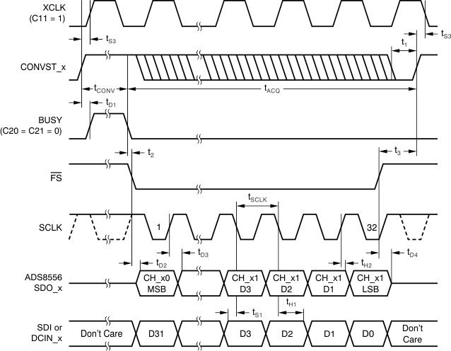
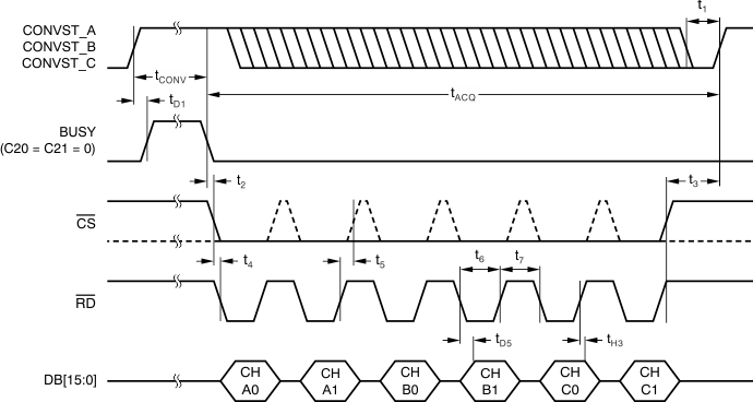
-
ADS855x 16-, 14-, 12-Bit, Six-Channel, Simultaneous Sampling Analog-to-Digital Converters
- 1 Features
- 2 Applications
- 3 Description
- 4 Revision History
- 5 Pin Configuration and Functions
-
6 Specifications
- 6.1 Absolute Maximum Ratings
- 6.2 ESD Ratings
- 6.3 Recommended Operating Conditions
- 6.4 Thermal Information
- 6.5 Electrical Characteristics: General
- 6.6 Electrical Characteristics: ADS8556
- 6.7 Electrical Characteristics: ADS8557
- 6.8 Electrical Characteristics: ADS8558
- 6.9 Power Dissipation Characteristics
- 6.10 Serial Interface Timing Requirements
- 6.11 Parallel Interface Timing Requirements (Read Access)
- 6.12 Parallel Interface Timing Requirements (Write Access)
- 6.13 Typical Characteristics
- 7 Detailed Description
- 8 Application and Implementation
- 9 Power Supply Recommendations
- 10Layout
- 11Device and Documentation Support
- 12Mechanical, Packaging, and Orderable Information
- IMPORTANT NOTICE
Package Options
Mechanical Data (Package|Pins)
- PM|64
Thermal pad, mechanical data (Package|Pins)
Orderable Information
ADS855x 16-, 14-, 12-Bit, Six-Channel, Simultaneous Sampling Analog-to-Digital Converters
1 Features
- Family of 16-, 14-, 12-Bit, Pin- and
Software-Compatible ADCs - Six SAR ADCs Grouped in Three Pairs
- Maximum Data Rate Per Channel with Internal Conversion Clock and Reference:
ADS8556: 630 kSPS (PAR) or 450 kSPS (SER)
ADS8557: 670 kSPS (PAR) or 470 kSPS (SER)
ADS8558: 730 kSPS (PAR) or 500 kSPS (SER) - Maximum Data Rate with External Conversion Clock and Reference:
800 kSPS (PAR) or 530 kSPS (SER) - Pin-Selectable or Programmable Input Voltage Ranges: Up to ±12 V
- Excellent Signal-to-Noise Performance:
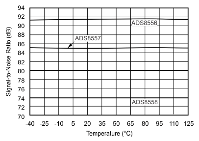
ADS8556: 91.5 dB, ADS8667: 85 dB,
ADS8668: 73.9 dB - Programmable and Buffered Internal Reference: 0.5 V to 2.5 V and 0.5 V to 3.0 V
- Comprehensive Power-Down Modes:
- Deep Power-Down (Standby Mode)
- Partial Power-Down
- Auto-Nap Power-Down
- Selectable Parallel or Serial Interface
- Operating Temperature Range: –40°C to 125°C
Block Diagram
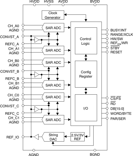
2 Applications
- Power Quality Measurement
- Protection Relays
- Multi-Axis Motor Control
- Programmable Logic Controllers
- Industrial Data Acquisition
3 Description
The ADS855x contains six low-power, 16-, 14-, or 12-bit, successive approximation register (SAR) based analog-to-digital converters (ADCs) with true bipolar inputs. Each channel contains a sample-and-hold circuit that allows simultaneous high-speed multi-channel signal acquisition.
The ADS855x supports data rates of up to 730 kSPS in parallel interface mode or up to 500 kSPS if the serial interface is used. The bus width of the parallel interface can be set to eight or 16 bits. In serial mode, up to three output channels can be activated.
The ADS855x is specified over the full industrial temperature range of –40°C to 125°C and is available in an LQFP-64 package.
Device Information(1)
| PART NUMBER | PACKAGE | BODY SIZE (NOM) |
|---|---|---|
| ADS8556 | LQFP (64) | 10.00 mm × 10.00 mm |
| ADS8557 | ||
| ADS8558 |
- For all available packages, see the orderable addendum at the end of the data sheet.
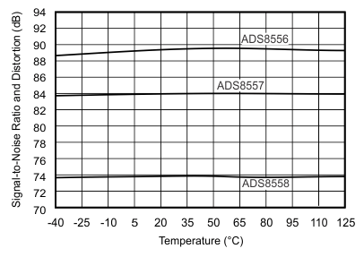
SNR vs Temperature
4 Revision History
Changes from C Revision (November 2015) to D Revision
- Moved Electrical Characteristics: General table to before other Electrical Characteristics tablesGo
- Added text reference for Figure 42 Go
- Changed Figure 43: changed capacitor values from 820 nF to 820 pFGo
Changes from B Revision (January 2012) to C Revision
- Added ESD Ratings table, Feature Description section, Device Functional Modes, Application and Implementation section, Power Supply Recommendations section, Layout section, Device and Documentation Support section, and Mechanical, Packaging, and Orderable Information section. Go
Changes from A Revision (August 2009) to B Revision
- Changed unit column for all tCONV rows in the Serial Interface Timing Requirements tableGo
- Added tS3 row to Serial Interface Timing Requirements tableGo
- Changed unit column for all tCONV rows in Parallel Interface Timing Requirements (Read Access) tableGo
- Updated Figure 2Go
- Updated Figure 3Go
- Changed second paragraph of CONVST_x sectionGo
- Changed minimum bandwidth value in last sentence of Reference sectionGo
- Updated Figure 38Go
5 Pin Configuration and Functions

Pin Functions
| PIN | TYPE(1) | DESCRIPTION | ||
|---|---|---|---|---|
| NAME | NO. | PARALLEL INTERFACE (PAR/SER = 0) | SERIAL INTERFACE (PAR/SER = 1) | |
| DB14/REFBUFEN | 1 | DIO, DI | Data bit 14 input/output Output is '0' for the ADS8557, ADS8558 |
Hardware mode (HW/SW = 0): Reference buffers enable input. When low, all reference buffers are enabled (mandatory if internal reference is used). When high, all reference buffers are disabled. |
| Software mode (HW/SW = 1): Connect to BGND or BVDD. The reference buffers are controlled by bit C24 (REFBUF) in control register (CR). |
||||
| DB13/SDI | 2 | DIO, DI | Data bit 13 input/output Output is MSB for the ADS8557 and '0' for the ADS8558 |
Hardware mode (HW/SW = 0): Connect to BGND |
| Software mode (HW/SW = 1): Serial data input |
||||
| DB12 | 3 | DIO | Data bit 12 input/output Output is '0' for the ADS8558 |
Connect to BGND |
| DB11 | 4 | DIO | Data bit 11 input/output Output is MSB for the ADS8558 |
Connect to BGND |
| DB10/SDO_C | 5 | DIO, DO | Data bit 10 input/output | When SEL_C = 1, data output for channel C When SEL_C = 0, tie this pin to BGND |
| DB9/SDO_B | 6 | DIO, DO | Data bit 9 input/output | When SEL_B = 1, data output for channel B When SEL_B = 0, tie this pin to BGND When SEL_C = 0, data from channel C1 are also available on this output |
| DB8/SDO_A | 7 | DIO, DO | Data bit 8 input/output | Data output for channel A When SEL_C = 0, data from channel C0 are also available on this output When SEL_C = 0 and SEL_B = 0, SDO_A acts as the single data output for all channels |
| BGND | 8 | P | Buffer IO ground, connect to digital ground plane | |
| BVDD | 9 | P | Buffer IO supply, connect to digital supply (2.7 V to 5.5 V). Decouple with a 1-μF ceramic capacitor or a combination of 100-nF and 10-μF ceramic capacitors to BGND. | |
| DB7/HBEN/DCEN | 10 | DIO, DI, DI | Word mode (WORD/BYTE = 0): Data bit 7 input/output | Daisy-chain enable input. When high, DB[5:3] serve as daisy-chain inputs DCIN[A:C]. If daisy-chain mode is not used, connect to BGND. |
| Byte mode (WORD/BYTE = 1): High byte enable input. When high, the high byte is output first on DB[15:8]. When low, the low byte is output first on DB[15:8]. |
||||
| DB6/SCLK | 11 | DIO, DI | Word mode (WORD/BYTE = 0): Data bit 6 input/output |
Serial interface clock input (36 MHz, max) |
| Byte mode (WORD/BYTE = 1): Connect to BGND or BVDD |
||||
| DB5/DCIN_A | 12 | DIO, DI | Word mode (WORD/BYTE = 0): Data bit 5 input/output |
When DCEN = 1, daisy-chain data input for channel A. When DCEN = 0, connect to BGND. |
| Byte mode (WORD/BYTE = 1): Connect to BGND or BVDD |
||||
| DB4/DCIN_B | 13 | DIO, DI | Word mode (WORD/BYTE = 0): Data bit 4 input/output |
When SEL_B = 1 and DCEN = 1, daisy-chain data input for channel B. When DCEN = 0, connect to BGND. |
| Byte mode (WORD/BYTE = 1): Connect to BGND or BVDD |
||||
| DB3/DCIN_C | 14 | DIO, DI | Word mode (WORD/BYTE = 0): Data bit 3 input/output |
When SEL_C = 1 and DCEN = 1, daisy-chain data input for channel C. When DCEN = 0, connect to BGND. |
| Byte mode (WORD/BYTE = 1): Connect to BGND or BVDD |
||||
| DB2/SEL_C | 15 | DIO, DI | Word mode (WORD/BYTE = 0): Data bit 2 input/output |
Select SDO_C input. When high, SDO_C is active. When low, SDO_C is disabled. |
| Byte mode (WORD/BYTE = 1): Connect to BGND or BVDD |
||||
| DB1/SEL_B | 16 | DIO, DI | Word mode (WORD/BYTE = 0): Data bit 1 input/output |
Select SDO_B input. When high, SDO_B is active. When low, SDO_B is disabled. |
| Byte mode (WORD/BYTE = 1): Connect to BGND or BVDD |
||||
| DB0/SEL_A | 17 | DIO, DI | Word mode (WORD/BYTE = 0): Data bit 0 (LSB) input/output |
Select SDO_A input. When high, SDO_A is active. When low, SDO_A is disabled. Must always be high. |
| Byte mode (WORD/BYTE = 1): Connect to BGND or BVDD |
||||
| BUSY/INT | 18 | DO | When CR bit C21 = 0 (BUSY/INT), converter busy status output. Transitions high when a conversion has been started and remains high during the entire process. Transitions low when the conversion data of all six channels are latched to the output register and remains low thereafter. In sequential mode (SEQ = 1 in the CR), the BUSY output transitions high when a conversion has been started and goes low for a single conversion clock cycle (tCCLK) whenever a channel pair conversion is completed. When bit C21 = 1 (BUSY/INT in CR), interrupt output. This bit transitions high after a conversion completes and remains high until the conversion result is read. The polarity of BUSY/INT output can be changed using bit C20 (BUSY L/H) in the control register. |
|
| CS/FS | 19 | DI, DI | Chip select input. When low, the parallel interface is enabled. When high, the interface is disabled. |
Frame synchronization. The falling edge of FS controls the frame transfer. |
| RD | 20 | DI | Read data input. When low, the parallel data output is enabled. When high, the data output is disabled. |
Connect to BGND. |
| CONVST_C | 21 | DI | Hardware mode (HW/SW = 0): Conversion start of channel pair C. The rising edge of this signal initiates simultaneous conversion of analog signals at inputs CH_C[1:0]. CONVST_C must remain high during the entire conversion cycle, otherwise both ADCs of channel C are put in partial power-down mode (see the Reset and Power-Down Modes section). |
|
| Software mode (HW/SW = 1): Conversion start of channel pair C in sequential mode (CR bit C23 = 1) only; connect to BGND or BVDD otherwise. | ||||
| CONVST_B | 22 | DI | Hardware mode (HW/SW = 0): Conversion start of channel pair B. The rising edge of this signal initiates simultaneous conversion of analog signals at inputs CH_B[1:0]. CONVST_B must remain high during the entire conversion cycle; otherwise, both ADCs of channel B are put into partial power-down mode (see the Reset and Power-Down Modes section). |
|
| Software mode (HW/SW = 1): Conversion start of channel pair B in sequential mode (CR bit C23 = 1) only; connect to BGND or BVDD otherwise. | ||||
| CONVST_A | 23 | DI | Hardware mode (HW/SW = 0): Conversion start of channel pair A. The rising edge of this signal initiates simultaneous conversion of analog signals at inputs CH_A[1:0]. CONVST_A must remain high during the entire conversion cycle; otherwise, both ADCs of channel A are put into partial power-down mode (see the Reset and Power-Down Modes section). |
|
| Software mode (HW/SW = 1): Conversion start of all selected channels except in sequential mode (CR bit C23 = 1): Conversion start of channel pair A only. |
||||
| STBY | 24 | DI | Standby mode input. When low, the entire device is powered-down (including the internal clock and reference). When high, the device operates in normal mode. |
|
| AGND | 25, 32, 37, 38, 43, 44, 49, 52, 53, 55, 57, 59 | P | Analog ground, connect to analog ground plane Pin 25 can have a dedicated ground if the difference between its potential and AGND is always kept within ±300 mV. |
|
| AVDD | 26, 34, 35, 40, 41, 46, 47, 50, 60 | P | Analog power supply (4.5 V to 5.5 V). Decouple each pin with a 100-nF ceramic capacitor to AGND. Use an additional 10-μF capacitor to AGND close to the device but without compromising the placement of the smaller capacitor. Pin 26 can have a dedicated power supply if the difference between its potential and AVDD is always kept within ±300 mV. | |
| RANGE/XCLK | 27 | DI, DIO | Hardware mode (HW/SW = 0): Input voltage range select input. When low, the analog input range is ±4 VREF. When high, the analog input range is ±2 VREF. |
|
| Software mode (HW/SW = 1): External conversion clock input, if CR bit C11 (CLKSEL) is set high or internal conversion clock output, if CR bit C10 (CLKOUT_EN) is set high. If not used, connect to BVDD or BGND. | ||||
| RESET | 28 | DI | Reset input, active high. Aborts any ongoing conversions. Resets the internal control register to 0x000003FF. The RESET pulse must be at least 50 ns long. | |
| WORD/BYTE | 29 | DI | Output mode selection input. When low, data are transferred in word mode using DB[15:0]. When high, data are transferred in byte mode using DB[15:8] with the byte order controlled by HBEN pin while two accesses are required for a complete 16-bit transfer. |
Connect to BGND. |
| HVSS | 30 | P | Negative supply voltage for the analog inputs (–16.5 V to –5 V). Decouple with a 100-nF ceramic capacitor to AGND placed next to the device and a 10-μF capacitor to AGND close to the device but without compromising the placement of the smaller capacitor. |
|
| HVDD | 31 | P | Positive supply voltage for the analog inputs (5 V to 16.5 V). Decouple with a 100-nF ceramic capacitor to AGND placed next to the device and a 10-μF capacitor to AGND close to the device but without compromising the placement of the smaller capacitor. | |
| CH_A0 | 33 | AI | Analog input of channel A0. The input voltage range is controlled by RANGE pin in hardware mode or CR bit C26 (RANGE_A) in software mode. | |
| CH_A1 | 36 | AI | Analog input of channel A1. The input voltage range is controlled by RANGE pin in hardware mode or CR bit C26 (RANGE_A) in software mode. | |
| CH_B0 | 39 | AI | Analog input of channel B0. The input voltage range is controlled by RANGE pin in hardware mode or CR bit C27 (RANGE_B) in software mode. | |
| CH_B1 | 42 | AI | Analog input of channel B1. The input voltage range is controlled by RANGE pin in hardware mode or CR bit C27 (RANGE_B) in software mode. | |
| CH_C0 | 45 | AI | Analog input of channel C0. The input voltage range is controlled by RANGE pin in hardware mode or CR bit C28 (RANGE_C) in software mode. | |
| CH_C1 | 48 | AI | Analog input of channel C1. The input voltage range is controlled by RANGE pin in hardware mode or CR bit C28 (RANGE_C) in software mode. | |
| REFIO | 51 | AIO | Reference voltage input/output (0.5 V to 3.025 V). The internal reference is enabled via REFEN/WR pin in hardware mode or CR bit C25 (REFEN) in software mode. The output value is controlled by the internal DAC (CR bits C[9:0]). Connect a 470-nF ceramic decoupling capacitor between this pin and pin 52. |
|
| REFC_A | 54 | AI | Decoupling capacitor for reference of channels A. Connect a 10-μF ceramic decoupling capacitor between this pin and pin 53. |
|
| REFC_B | 56 | AI | Decoupling capacitor for reference of channels B. Connect a 10-μF ceramic decoupling capacitor between this pin and pin 55. |
|
| REFC_C | 58 | AI | Decoupling capacitor for reference of channels C. Connect a 10-μF ceramic decoupling capacitor between this pin and pin 57. |
|
| PAR/SER | 61 | DI | Interface mode selection input. When low, the parallel interface is selected. When high, the serial interface is enabled. |
|
| HW/SW | 62 | DI | Mode selection input. When low, the hardware mode is selected and part works according to the settings of external pins. When high, the software mode is selected in which the device is configured by writing into the control register. |
|
| REFEN/WR | 63 | DI | Hardware mode (HW/SW = 0): Internal reference enable input. When high, the internal reference is enabled (the reference buffers are to be enabled). When low, the internal reference is disabled and an external reference is applied at REFIO. |
Hardware mode (HW/SW = 0): Internal reference enable input. When high, the internal reference is enabled (the reference buffers are to be enabled). When low, the internal reference is disabled and an external reference must be applied at REFIO. |
| Software mode (HW/SW = 1): Write input. The parallel data input is enabled, when CS and WR are low. The internal reference is enabled by the CR bit C25 (REFEN). |
Software mode (HW/SW = 1): Connect to BGND or BVDD. The internal reference is enabled by CR bit C25 (REFEN). |
|||
| DB15 | 64 | DIO | Data bit 15 (MSB) input/output. Output is '0' for the ADS8557/8. |
Connect to BGND. |
6 Specifications
6.1 Absolute Maximum Ratings
over operating free-air temperature range (unless otherwise noted)(1)| MIN | MAX | UNIT | |
|---|---|---|---|
| Supply voltage, HVDD to AGND | –0.3 | 18 | V |
| Supply voltage, HVSS to AGND | –18 | 0.3 | V |
| Supply voltage, AVDD to AGND | –0.3 | 6 | V |
| Supply voltage, BVDD to BGND | –0.3 | 6 | V |
| Analog input voltage | HVSS – 0.3 | HVDD + 0.3 | V |
| Reference input voltage with respect to AGND | AGND – 0.3 | AVDD + 0.3 | V |
| Digital input voltage with respect to BGND | BGND – 0.3 | BVDD + 0.3 | V |
| Ground voltage difference AGND to BGND | ±0.3 | V | |
| Input current to all pins except supply | –10 | 10 | mA |
| Maximum virtual junction temperature, TJ | 150 | °C | |
| Storage Temperature, Tstg | -65 | 150 | °C |
6.2 ESD Ratings
| VALUE | UNIT | |||
|---|---|---|---|---|
| V(ESD) | Electrostatic discharge | Human-body model (HBM), per ANSI/ESDA/JEDEC JS-001 JEDEC standard 22, test method A114-C.01(1) |
±2000 | V |
| Charged-device model (CDM), per JEDEC specification JESD22-C101 JEDEC standard 22, test method C101(2) |
±500 | |||
6.3 Recommended Operating Conditions
| MIN | NOM | MAX | UNIT | ||
|---|---|---|---|---|---|
| Supply voltage, AVDD to AGND | 4.5 | 5 | 5.5 | V | |
| Supply voltage, BVDD to BGND | Low-voltage levels | 2.7 | 3.0 | 3.6 | V |
| 5-V logic levels | 4.5 | 5 | 5.5 | ||
| Input supply voltage, HVDD to AGND | Range 1 (±2 × VREF) | 2 × VREF | 16.5 | V | |
| Range 2 (±4 × VREF) | 4 × VREF | 16.5 | |||
| Input supply voltage, HVSS to AGND | Range 1 (±2 × VREF) | –16.5 | –2 × VREF | V | |
| Range 2 (±4 × VREF) | –16.5 | –4 × VREF | |||
| Reference input voltage (VREF) | 0.5 | 2.5 | 3.0 | V | |
| Analog inputs(1) | Range 1 (±2 × VREF) | –2 × VREF | 2 × VREF | V | |
| Range 1 (±4 × VREF) | –4 × VREF | 4 × VREF | |||
| Operating ambient temperature, TA | –40 | 125 | °C | ||
6.4 Thermal Information
| THERMAL METRIC(1) | ADS855x | UNIT | ||
|---|---|---|---|---|
| PM (LQFP) | ||||
| 64 PINS | ||||
| RθJA | Junction-to-ambient thermal resistance | High-K thermal resistance(2) | 50.3 | °C/W |
| RθJC(top) | Junction-to-case (top) thermal resistance | 12.0 | °C/W | |
| RθJB | Junction-to-board thermal resistance | 24.0 | °C/W | |
| ψJT | Junction-to-top characterization parameter | 0.5 | °C/W | |
| ψJB | Junction-to-board characterization parameter | 23.5 | °C/W | |
| RθJC(bot) | Junction-to-case (bottom) thermal resistance | NA | °C/W | |
6.5 Electrical Characteristics: General
over recommended operating free-air temperature range of –40°C to 125°C, AVDD = 4.5 V to 5.5 V, BVDD = 2.7 V to 5.5 V, HVDD = 10 V to 15 V, HVSS = –15 V to –10 V, VREF = 2.5 V (internal), and fDATA = maximum (unless otherwise noted)| PARAMETER | TEST CONDITIONS | MIN | TYP(1) | MAX | UNIT | |
|---|---|---|---|---|---|---|
| ANALOG INPUT | ||||||
| CHXX | Bipolar full-scale range | RANGE pin/RANGE bit = 0 | –4 × VREF | 4 × VREF | V | |
| RANGE pin/RANGE bit = 1 | –2 × VREF | 2 × VREF | ||||
| Input capacitance | Input range = ±4 × VREF | 10 | pF | |||
| Input range = ±2 × VREF | 20 | |||||
| Input leakage current | No ongoing conversion | ±1 | μA | |||
| Aperture delay | 5 | ns | ||||
| Aperture delay matching | Common CONVST for all channels | 250 | ps | |||
| Aperture jitter | 50 | ps | ||||
| EXTERNAL CLOCK INPUT (XCLK) | ||||||
| fXCLK | External clock frequency | An external reference must be used for fXCLK > fCCLK | 1 | 18 | 20 | MHz |
| External clock duty cycle | 45% | 55% | ||||
| REFERENCE VOLTAGE OUTPUT (REFOUT) | ||||||
| VREF | Reference voltage | 2.5-V operation, REFDAC = 0x3FF | 2.485 | 2.5 | 2.515 | V |
| 2.5-V operation, REFDAC = 0x3FF at 25°C | 2.496 | 2.5 | 2.504 | |||
| 3-V operation, REFDAC = 0x3FF | 2.985 | 3.0 | 3.015 | |||
| 3-V operation, REFDAC = 0x3FF at 25°C | 2.995 | 3.0 | 3.005 | |||
| dVREF/dT | Reference voltage drift | ±10 | ppm/°C | |||
| PSRR | Power-supply rejection ratio | 73 | dB | |||
| IREFOUT | Output current | With dc current | –2 | 2 | mA | |
| IREFSC | Short-circuit current(2) | 50 | mA | |||
| tREFON | Turn-on settling time | 10 | ms | |||
| External load capacitance | At CREF_x pins | 4.7 | 10 | μF | ||
| At REFIO pins | 100 | 470 | ||||
| REFDAC | Tuning range | Internal reference output voltage range | 0.2 × VREF | VREF | V | |
| REFDAC resolution | 10 | Bits | ||||
| DNLDAC | REFDAC differential nonlinearity | –1 | ±0.1 | 1 | LSB | |
| INLDAC | REFDAC integral nonlinearity | –2 | ±0.1 | 2 | LSB | |
| VOSDAC | REFDAC offset error | VREF = 0.5 V (DAC = 0x0CC) | –4 | ±0.65 | 4 | LSB |
| REFERENCE VOLTAGE INPUT (REFIN) | ||||||
| VREFIN | Reference input voltage | 0.5 | 2.5 | 3.025 | V | |
| Input resistance | 100 | MΩ | ||||
| Input capacitance | 5 | pF | ||||
| Reference input current | 1 | μA | ||||
| SERIAL CLOCK INPUT (SCLK) | ||||||
| fSCLK | Serial clock input frequency | 0.1 | 36 | MHz | ||
| tSCLK | Serial clock period | 0.0278 | 10 | μs | ||
| Serial clock duty cycle | 40% | 60% | ||||
| DIGITAL INPUTS(3) | ||||||
| Logic family | CMOS with Schmitt-Trigger | |||||
| High-level input voltage | 0.7 × BVDD | BVDD + 0.3 | V | |||
| Low-level input voltage | BGND – 0.3 | 0.3 × BVDD | V | |||
| Input current | VI = BVDD to BGND | –50 | 50 | nA | ||
| Input capacitance | 5 | pF | ||||
| DIGITAL OUTPUTS(3) | ||||||
| Logic family | CMOS | |||||
| High-level output voltage | IOH = 100 μA | BVDD – 0.6 | BVDD | V | ||
| Low-level output voltage | IOH = –100 μA | BGND | BGND + 0.4 | V | ||
| High-impedance-state output current | –50 | 50 | nA | |||
| Output capacitance | 5 | pF | ||||
| Load capacitance | 30 | pF | ||||
| POWER-SUPPLY REQUIREMENTS | ||||||
| AVDD | Analog supply voltage | 4.5 | 5 | 5.5 | V | |
| BVDD | Buffer I/O supply voltage | 2.7 | 3 | 5.5 | V | |
| HVDD | Input positive supply voltage | 5 | 10 | 16.5 | V | |
| HVSS | Input negative supply voltage | –16.5 | –10 | –5 | V | |
| IAVDD | Analog supply current(4) | fDATA = maximum | 30 | 36 | mA | |
| ADS8556, fDATA = 250 kSPS (auto-NAP mode) | 14 | 16.5 | ||||
| ADS8557, fDATA = 250 kSPS (auto-NAP mode) | 14 | 17 | ||||
| ADS8558, fDATA = 250 kSPS (auto-NAP mode) | 14 | 18 | ||||
| Auto-NAP mode, no ongoing conversion, internal conversion clock | 4 | 6 | ||||
| Power-down mode | 0.1 | 50 | μA | |||
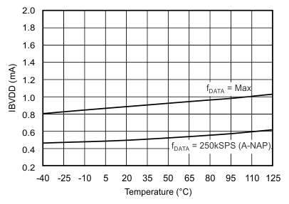
| IBVDD | Buffer I/O supply current(5) | fDATA = maximum | 0.9 | 2 | mA | |
| fDATA = 250 kSPS (auto-NAP mode) | 0.5 | 1.5 | ||||
| Auto-NAP mode, no ongoing conversion, internal conversion clock | 0.1 | 10 | μA | |||
| Power-down mode | 0.1 | 10 | ||||
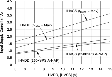
| IHVDD | Input positive supply current(6) | ADS8556, fDATA = maximum | 3 | 3.5 | mA | |
| ADS8557, fDATA = maximum | 3.1 | 3.6 | ||||
| ADS8558, fDATA = maximum | 3.3 | 4 | ||||
| fDATA = 250 kSPS (auto-NAP mode) | 1.6 | 2 | ||||
| Auto-NAP mode, no ongoing conversion, internal conversion clock | 0.2 | 0.3 | μA | |||
| Power-down mode | 0.1 | 10 | ||||
| IHVSS | Input negative supply current(7) | ADS8556, fDATA = maximum | 3.6 | 4 | mA | |
| ADS8557, fDATA = maximum | 3.6 | 4.2 | ||||
| ADS8558, fDATA = maximum | 4 | 4.8 | ||||
| fDATA = 250 kSPS (auto-NAP mode) | 1.8 | 2.2 | ||||
| Auto-NAP mode, no ongoing conversion, internal conversion clock | 0.2 | 0.25 | μA | |||
| Power-down mode | 0.1 | 10 | ||||
| Power dissipation(8) | ADS8556, fDATA = maximum | 251.7 | 298.5 | mW | ||
| ADS8557, fDATA = maximum | 253.2 | 303 | ||||
| ADS8558, fDATA = maximum | 262.2 | 318 | ||||
| ADS8556, fDATA = 250 kSPS (auto-NAP mode) | 122.5 | 150 | ||||
| ADS8557, fDATA = 250 kSPS (auto-NAP mode) | 122.5 | 152.5 | ||||
| ADS8558, fDATA = 250 kSPS (auto-NAP mode) | 122.5 | 157.5 | ||||
| Auto-NAP mode, no ongoing conversion, internal conversion clock | 26 | 38.3 | ||||
| Power-down mode | 3.8 | 580 | μW | |||
6.6 Electrical Characteristics: ADS8556
over recommended operating free-air temperature range of –40°C to 125°C, AVDD = 4.5 V to 5 V, BVDD = 2.7 V to 5.5 V, HVDD = 10 V to 15 V, HVSS = –15 V to –10 V, VREF = 2.5 V (internal), and fDATA = 630 kSPS in parallel mode or 450 kSPS in serial mode (unless otherwise noted)| PARAMETER | TEST CONDITIONS | MIN | TYP(1) | MAX | UNIT | |
|---|---|---|---|---|---|---|
| DC ACCURACY | ||||||
| Resolution | 16 | Bits | ||||
| No missing codes | 16 | Bits | ||||
| INL | Integral linearity error | At TA = –40°C to 85°C | –3 | ±1.5 | 3 | LSB |
| At TA = –40°C to 125°C | –4 | ±1.5 | 4 | |||
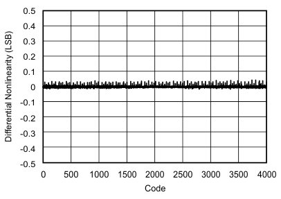
| DNL | Differential linearity error | At TA = –40°C to 85°C | –1 | ±0.75 | 1.5 | LSB |
| At TA = –40°C to 125°C | –1 | ±0.75 | 2 | |||
| Offset error | –4 | ±0.8 | 4 | mV | ||
| Offset error drift | ±3.5 | μV/°C | ||||
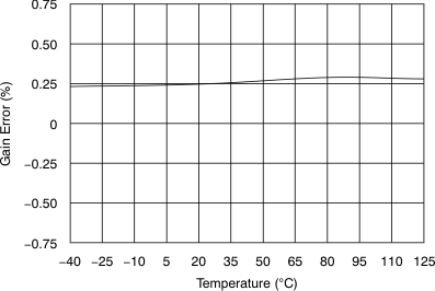
| Gain error | Referenced to voltage at REFIO | –0.75 | ±0.25 | 0.75 | %FSR | |
| Gain error drift | Referenced to voltage at REFIO | ±6 | ppm/°C | |||
| PSRR | Power-supply rejection ratio | At output code FFFFh, related to AVDD | 60 | dB | ||
| SAMPLING DYNAMICS | ||||||
| tACQ | Acquisition time | 280 | ns | |||
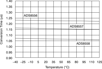
| tCONV | Conversion time per ADC | 1.26 | μs | |||
| tCCLK | Internal conversion clock period | 18.5 | tCCLK | |||
| 68.0 | ns | |||||
| fDATA | Throughput rate | Parallel interface, internal clock and reference | 630 | kSPS | ||
| Serial interface, internal clock and reference | 450 | |||||
| AC ACCURACY | ||||||
| SNR | Signal-to-noise ratio | At fIN = 10 kHz, TA = –40°C to 85°C | 90 | 91.5 | dB | |
| At fIN = 10 kHz, TA = –40°C to 125°C | 89 | 91.5 | ||||
| SINAD | Signal-to-noise ratio + distortion | At fIN = 10 kHz, TA = –40°C to 85°C | 87 | 89.5 | dB | |
| At fIN = 10 kHz, TA = –40°C to 125°C | 86.5 | 89.5 | ||||
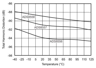
| THD | Total harmonic distortion(2) | At fIN = 10 kHz, TA = –40°C to 85°C | –94 | –90 | dB | |
| At fIN = 10 kHz, TA = –40°C to 125°C | –94 | –89.5 | ||||
| SFDR | Spurious-free dynamic range | At fIN = 10 kHz, TA = –40°C to 85°C | 90 | 95 | dB | |
| At fIN = 10 kHz, TA = –40°C to 125°C | 89.5 | 95 | ||||
| Channel-to-channel isolation | At fIN = 10 kHz | 100 | dB | |||
| –3-dB small-signal bandwidth | In 4 × VREF mode | 48 | MHz | |||
| In 2 × VREF mode | 24 | |||||
6.7 Electrical Characteristics: ADS8557
over recommended operating free-air temperature range of –40°C to 125°C, AVDD = 4.5 V to 5.5 V, BVDD = 2.7 V to 5.5 V, HVDD = 10 V to 15 V, HVSS = –15 V to –10 V, VREF = 2.5 V (internal), and fDATA = 670 kSPS in parallel mode or 470 kSPS in serial mode (unless otherwise noted)| PARAMETER | TEST CONDITIONS | MIN | TYP(1) | MAX | UNIT | |
|---|---|---|---|---|---|---|
| DC ACCURACY | ||||||
| Resolution | 14 | Bits | ||||
| No missing codes | 14 | Bits | ||||
| INL | Integral linearity error | –1 | ±0.4 | 1 | LSB | |
| DNL | Differential linearity error | –1 | ±0.25 | 1 | LSB | |
| Offset error | –4 | ±0.8 | 4 | mV | ||
| Offset error drift | ±3.5 | μV/°C | ||||
| Gain error | Referenced to voltage at REFIO | –0.75 | ±0.25 | 0.75 | %FSR | |
| Gain error drift | Referenced to voltage at REFIO | ±6 | ppm/°C | |||
| PSRR | Power-supply rejection ratio | At output code FFFFh, related to AVDD | 60 | dB | ||
| SAMPLING DYNAMICS | ||||||
| tACQ | Acquisition time | 280 | ns | |||
| tCONV | Conversion time per ADC | 1.19 | μs | |||
| tCCLK | Internal conversion clock period | 18.5 | tCCLK | |||
| 64.1 | ns | |||||
| fDATA | Throughput rate | Parallel interface, internal clock and reference | 670 | kSPS | ||
| Serial interface, internal clock and reference | 470 | |||||
| AC ACCURACY | ||||||
| SNR | Signal-to-noise ratio | At fIN = 10 kHz | 84 | 85 | dB | |
| SINAD | Signal-to-noise ratio + distortion | At fIN = 10 kHz | 83 | 84 | dB | |
| THD | Total harmonic distortion(2) | At fIN = 10 kHz | –91 | –86 | dB | |
| SFDR | Spurious-free dynamic range | At fIN = 10 kHz | 86 | 92 | dB | |
| Channel-to-channel isolation | At fIN = 10 kHz | 100 | dB | |||
| –3-dB small-signal bandwidth | In 4 × VREF mode | 48 | MHz | |||
| In 2 × VREF mode | 24 | |||||
6.8 Electrical Characteristics: ADS8558
over recommended operating free-air temperature range of –40°C to 125°C, AVDD = 4.5 V to 5 V, BVDD = 2.7 V to 5.5 V, HVDD = 10 V to 15 V, HVSS = –15 V to –10 V, VREF = 2.5 V (internal), and fDATA = 730 kSPS in parallel mode or 500 kSPS in serial mode (unless otherwise noted)| PARAMETER | TEST CONDITIONS | MIN | TYP(1) | MAX | UNIT | |
|---|---|---|---|---|---|---|
| DC ACCURACY | ||||||
| Resolution | 12 | Bits | ||||
| No missing codes | 12 | Bits | ||||
| INL | Integral linearity error | –0.75 | ±0.2 | 0.75 | LSB | |
| DNL | Differential linearity error | –0.5 | ±0.2 | 0.5 | LSB | |
| Offset error | –4 | ±0.8 | 4 | mV | ||
| Offset error drift | ±3.5 | μV/°C | ||||
| Gain error | Referenced to voltage at REFIO | –0.75 | ±0.25 | 0.75 | %FSR | |
| Gain error drift | Referenced to voltage at REFIO | ±6 | ppm/°C | |||
| PSRR | Power-supply rejection ratio | At output code FFFFh, related to AVDD | 60 | dB | ||
| SAMPLING DYNAMICS | ||||||
| tACQ | Acquisition time | 280 | ns | |||
| tCONV | Conversion time per ADC | 1.09 | μs | |||
| tCCLK | Internal conversion clock period | 18.5 | tCCLK | |||
| 58.8 | ns | |||||
| fDATA | Throughput rate | Parallel interface, internal clock and reference | 730 | kSPS | ||
| Serial interface, internal clock and reference | 500 | |||||
| AC ACCURACY | ||||||
| SNR | Signal-to-noise ratio | At fIN = 10kHz | 73 | 73.9 | dB | |
| SINAD | Signal-to-noise ratio + distortion | At fIN = 10kHz | 73 | 73.8 | dB | |
| THD | Total harmonic distortion(2) | At fIN = 10kHz | –89 | –84 | dB | |
| SFDR | Spurious-free dynamic range | At fIN = 10kHz | 84 | 92 | dB | |
| Channel-to-channel isolation | At fIN = 10kHz | 100 | dB | |||
| –3-dB small-signal bandwidth | In 4 × VREF mode | 48 | MHz | |||
| In 2 × VREF mode | 24 | |||||
6.9 Power Dissipation Characteristics
over operating free-air temperature range (unless otherwise noted)6.10 Serial Interface Timing Requirements
over recommended operating free-air temperature range at –40°C to 125°C, AVDD = 5 V, and BVDD = 2.7 V to 5.5 V (unless otherwise noted)(1)6.11 Parallel Interface Timing Requirements (Read Access)
over recommended operating free-air temperature range at –40°C to 125°C, AVDD = 5 V, and BVDD = 2.7 V to 5.5 V (unless otherwise noted)(1)| MIN | NOM | MAX | UNIT | |||
|---|---|---|---|---|---|---|
| tACQ | Acquisition time | 280 | ns | |||
| tCONV | Conversion time | ADS8556 | 1.26 | µs | ||
| ADS8557 | 1.19 | |||||
| ADS8558 | 1.09 | |||||
| t1 | CONVST_x low time | 20 | ns | |||
| t2 | BUSY low to CS low time | 0 | ns | |||
| t3 | Bus access finished to next conversion start time(2) | ADS8556 | 40 | ns | ||
| ADS8557 | 20 | |||||
| ADS8558 | 0 | |||||
| t4 | CS low to RD low time | 0 | ns | |||
| t5 | RD high to CS high time | 0 | ns | |||
| t6 | RD pulse duration | 30 | ns | |||
| t7 | Minimum time between two read accesses | 10 | ns | |||
| tD1 | CONVST_x high to BUSY high delay | 5 | 20 | ns | ||
| tD5 | RD falling edge to output data valid delay | 20 | ns | |||
| tH3 | Output data to RD rising edge hold time | 5 | ns | |||
6.12 Parallel Interface Timing Requirements (Write Access)
over recommended operating free-air temperature range at –40°C to 125°C, AVDD = 5 V, and BVDD = 2.7 V to 5.5 V (unless otherwise noted)(1)| MIN | NOM | MAX | UNIT | ||
|---|---|---|---|---|---|
| t8 | CS low to WR low time | 0 | ns | ||
| t9 | WR low pulse duration | 15 | ns | ||
| t10 | WR high pulse duration | 10 | ns | ||
| t11 | WR high to CS high time | 0 | ns | ||
| tS2 | Output data to WR rising edge setup time | 5 | ns | ||
| tH4 | Data output to WR rising edge hold time | 5 | ns | ||
 Figure 1. Equivalent Input Circuits
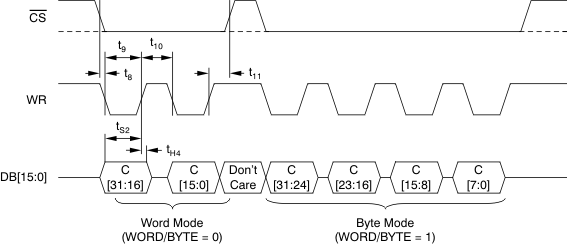 Figure 4. Parallel Write Access Timing Diagram
6.13 Typical Characteristics
at 25°C, over entire supply voltage range, VREF = 2.5 V (internal), and fDATA = maximum (unless otherwise noted)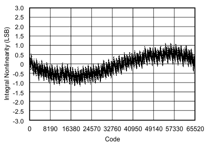
| AVDD = BVDD = 5 V | HVSS = –15 V | HVDD = 15 V |
| fDATA = max | Internal reference |

| AVDD = BVDD = 5 V | HVSS = –15 V | HVDD = 15 V |
| fDATA = max | Internal reference |
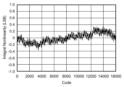
| AVDD = BVDD = 5 V | HVSS = –15 V | HVDD = 15 V |
| fDATA = max | Internal reference |
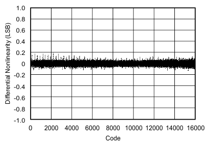
| AVDD = BVDD = 5 V | HVSS = –15 V | HVDD = 15 V |
| fDATA = max | Internal reference |
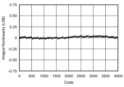
| AVDD = BVDD = 5 V | HVSS = –15 V | HVDD = 15 V |
| fDATA = max | Internal reference |
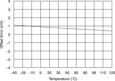
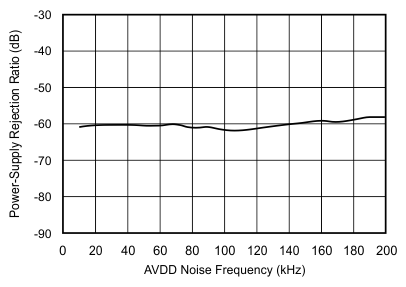
| CSUPPLY = 100 nF on AVDD | ||
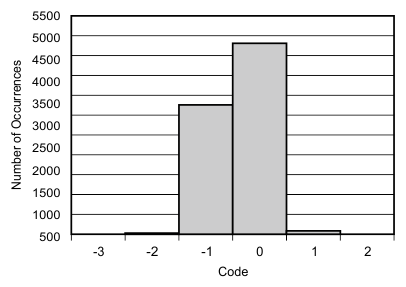
| AVDD = BVDD = 5 V | HVSS = –15 V | HVDD = 15 V |
| Range = 4 × VREF | 8192 samples | Internal reference |
| AVDD = BVDD = 5 V | HVSS = –15 V | HVDD = 15 V |
| Range = ±4 × VREF | fSIGNAL = 10 kHz | fDATA = max |
| Internal reference |
| AVDD = BVDD = 5 V | HVSS = –15 V | HVDD = 15 V |
| Range = ±4 × VREF | fSIGNAL = 10 kHz | fDATA = max |
| Internal reference |
| AVDD = BVDD = 5 V | fSAMPLE = 500 kSPS | HVSS = –15 V |
| Range = ±2 × VREF | fSIGNAL = 10 kHz | HVDD = 15 V |
| Internal reference |
(2048-Point FFT, fIN = 10 kHz, ±5-VIN Range)
Analog Supply Voltage (2.5-V Mode)
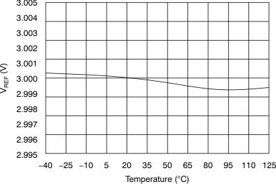
Temperature (3-V Mode)
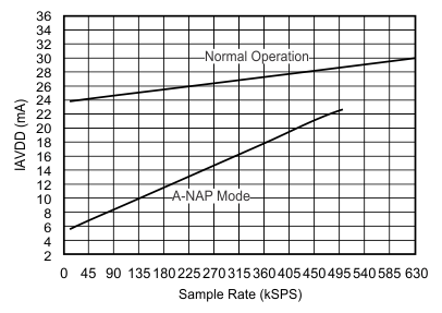
| AVDD = 5 V | Internal reference |
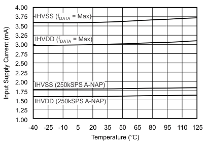
| Range = ±4 × VREF | HVSS = –15 V | HVDD = 15 V |
| Internal reference |
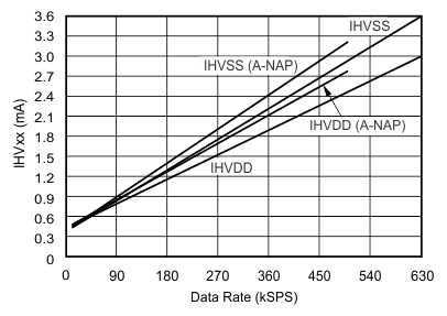
| Range = ±4 × VREF | HVSS = –15 V | HVDD = 15 V |
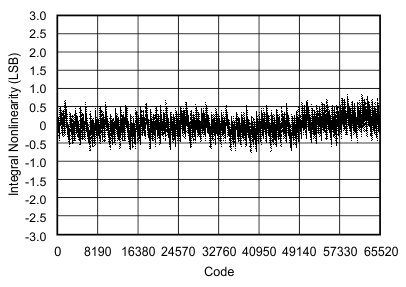
| AVDD = BVDD = 5 V | HVSS = –15 V | HVDD = 15 V |
| fDATA = max | Internal reference |
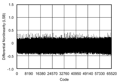
| AVDD = BVDD = 5 V | HVSS = –15 V | HVDD = 15 V |
| fDATA = max | Internal reference |
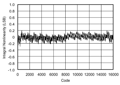
| AVDD = BVDD = 5 V | HVSS = –15 V | HVDD = 15 V |
| fDATA = max | Internal reference |
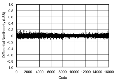
| AVDD = BVDD = 5 V | HVSS = –15 V | HVDD = 15 V |
| fDATA = max | Internal reference |
| AVDD = BVDD = 5 V | HVSS = –15 V | HVDD = 15 V |
| fDATA = max | Internal reference |

| AVDD = BVDD = 5 V | HVSS = –15 V | HVDD = 15 V |
| Range = ±4 × VREF | fSIGNAL = 10 kHz | fDATA = max |
| Internal reference |
| AVDD = BVDD = 5 V | HVSS = –15 V | HVDD = 15 V |
| Range = ±4 × VREF | fSIGNAL = 10 kHz | fDATA = max |
| Internal reference |
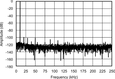
| AVDD = BVDD = 5 V | fSAMPLE = 500 kSPS | HVSS = –15 V |
| Range = ±4 × VREF | fSIGNAL = 10 kHz | HVDD = 15 V |
| Internal reference |
(2048-Point FFT, fIN = 10 kHz, ±10-VIN Range)
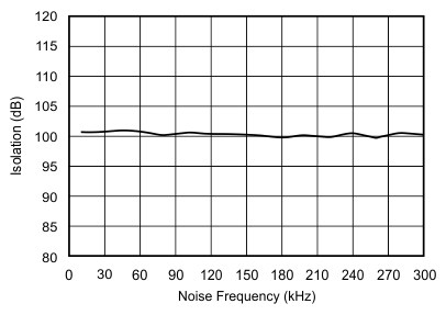
| AVDD = BVDD = 5 V | HVSS = –15 V | HVDD = 15 V |
| Range = ±2 × VREF | fDATA = max | Internal reference |
Input Noise Frequency
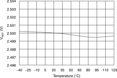
Temperature (2.5-V Mode)
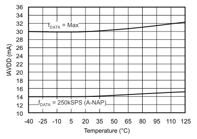
| AVDD = 5 V | Internal reference |
| BVDD = 5 V |
Input Supply Voltage
