SBAS633E February 2016 – August 2022 ADS8681 , ADS8685 , ADS8689
PRODUCTION DATA
- 1 Features
- 2 Applications
- 3 Description
- 4 Revision History
- 5 Pin Configuration and Functions
-
6 Specifications
- 6.1 Absolute Maximum Ratings
- 6.2 ESD Ratings
- 6.3 Recommended Operating Conditions
- 6.4 Thermal Information
- 6.5 Electrical Characteristics
- 6.6 Timing Requirements: Conversion Cycle
- 6.7 Timing Requirements: Asynchronous Reset
- 6.8 Timing Requirements: SPI-Compatible Serial Interface
- 6.9 Timing Requirements: Source-Synchronous Serial Interface (External Clock)
- 6.10 Timing Requirements: Source-Synchronous Serial Interface (Internal Clock)
- 6.11 Timing Diagrams
- 6.12 Typical Characteristics
-
7 Detailed Description
- 7.1 Overview
- 7.2 Functional Block Diagram
- 7.3 Feature Description
- 7.4 Device Functional Modes
- 7.5 Programming
- 7.6
Register Maps
- 7.6.1
Device Configuration and Register Maps
- 7.6.1.1 DEVICE_ID_REG Register (address = 00h)
- 7.6.1.2 RST_PWRCTL_REG Register (address = 04h)
- 7.6.1.3 SDI_CTL_REG Register (address = 08h)
- 7.6.1.4 SDO_CTL_REG Register (address = 0Ch)
- 7.6.1.5 DATAOUT_CTL_REG Register (address = 10h)
- 7.6.1.6 RANGE_SEL_REG Register (address = 14h)
- 7.6.1.7 ALARM_REG Register (address = 20h)
- 7.6.1.8 ALARM_H_TH_REG Register (address = 24h)
- 7.6.1.9 ALARM_L_TH_REG Register (address = 28h)
- 7.6.1
Device Configuration and Register Maps
- 8 Application and Implementation
- 9 Device and Documentation Support
- 10Mechanical, Packaging, and Orderable Information
Package Options
Refer to the PDF data sheet for device specific package drawings
Mechanical Data (Package|Pins)
- PW|16
- RUM|16
Thermal pad, mechanical data (Package|Pins)
Orderable Information
7.5.4.1 Protocols for Configuring the Device
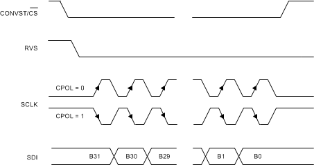
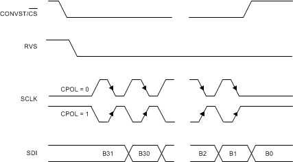
As described in Table 7-8, the host controller can use any of the four legacy, SPI-compatible protocols (SPI-00-S, SPI-01-S, SPI-10-S, or SPI-11-S) to write data into the device.
| PROTOCOL | SCLK POLARITY (At CS Falling Edge) |
SCLK PHASE (Capture Edge) |
SDI_CTL_REG | SDO_CTL_REG | DIAGRAM |
|---|---|---|---|---|---|
| SPI-00-S | Low | Rising | 00h | 00h | Figure 7-30 |
| SPI-01-S | Low | Falling | 01h | 00h | Figure 7-30 |
| SPI-10-S | High | Falling | 02h | 00h | Figure 7-31 |
| SPI-11-S | High | Rising | 03h | 00h | Figure 7-31 |
On power-up or after coming out of any asynchronous reset, the device supports the SPI-00-S protocol for data read and data write operations. To select a different SPI-compatible protocol, program the SDI_MODE[1:0] bits in the SDI_CNTL_REG register. This first write operation must adhere to the SPI-00-S protocol. Any subsequent data transfer frames must adhere to the newly-selected protocol. The SPI protocol selected by the configuration of the SDI_MODE[1:0] is applicable to both read and write operations.
Figure 7-30 and Figure 7-31 detail the four protocols using an optimal data frame; see the Section 6.8 table for associated timing parameters.
As explained in the Section 7.5.1 section, a valid write operation to the device requires a minimum of 32 SCLKs to be provided within a data transfer frame.

