at TA = 25°C, AVDD = 5V, DVDD = 3V,
VREF = 4.096V (internal), and maximum throughput (unless otherwise
noted)
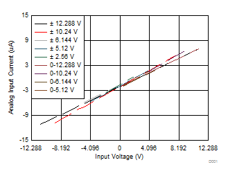
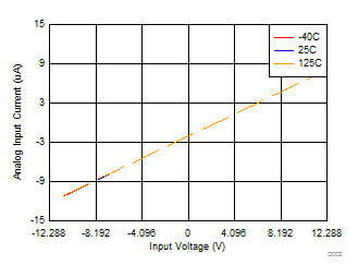
 Figure 5-9 Input
I-V Characteristic Across Input Ranges
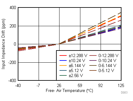
 Figure 5-11 Input
Impedance Drift vs Temperature
| Mean
= 32767.5, sigma = 2.87, input = 0V |
Figure 5-13 DC Histogram for Midscale
Inputs (±12.288V)
| Mean
= 32767.5, sigma = 2.87, input = 0V |
Figure 5-15 DC
Histogram for Midscale Inputs (±6.144V)
| Mean
= 32769.22, sigma = 2.87, input = 0V |
Figure 5-17 DC
Histogram for Midscale Inputs (±2.56V)
| Mean
= 32768.41, sigma = 3.1, input = 5.12V |
Figure 5-19 DC
Histogram for Midscale Inputs (0V–10.24V)
| Mean
= 32768.32, sigma = 3.16, input = 2.56V |
Figure 5-21 DC
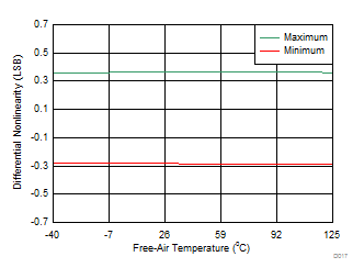
Histogram for Midscale Inputs (0V–5.12V) Figure 5-23 DNL
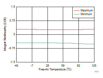
vs Temperature
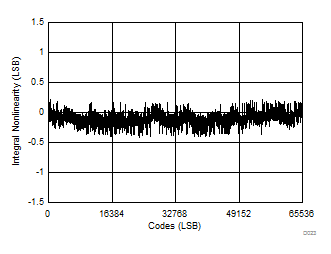
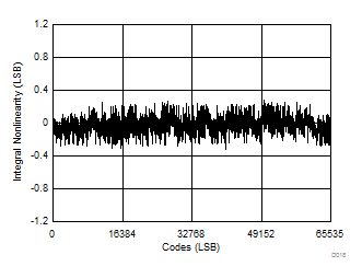
 Figure 5-25 Typical INL for All Codes (All Unipolar Ranges)
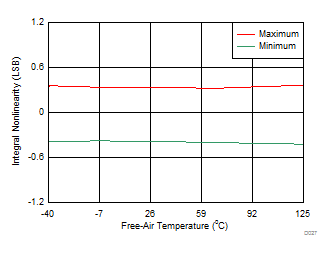
 Figure 5-27 INL
vs Temperature (All Unipolar Ranges)
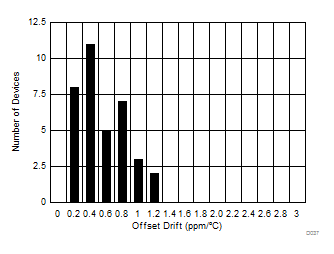
 Figure 5-29 Typical Histogram for Offset Drift
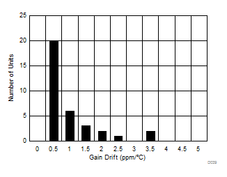
 Figure 5-31 Typical Histogram for Gain Error Drift
| Number of points = 500k, fIN = 1kHz |
Figure 5-33 Typical FFT Plot (All Ranges) for the ADS8681W
| Number of points = 500k, fIN = 1kHz |
Figure 5-35 Typical FFT Plot (All Ranges) for the ADS8689W Figure 5-37 SINAD
vs Input Frequency
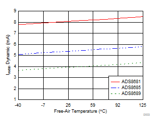
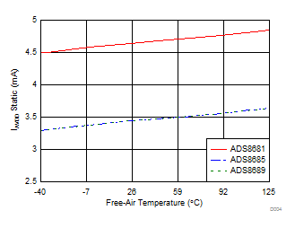
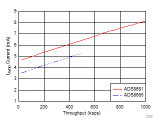
 Figure 5-39 AVDD
Current vs Temperature
 Figure 5-41 AVDD
Current vs Temperature (During Sampling)
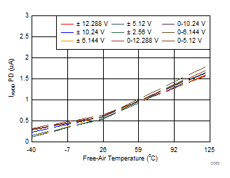
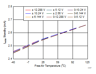
 Figure 5-43 AVDD
Current vs Temperature (Power-Down Mode)
 Figure 5-10 Input I-V Characteristic
Across Temperature
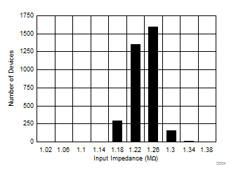
 Figure 5-12 Typical Distribution of Input Impedance
| Mean
= 32767.24, sigma = 2.87, input = 0V |
Figure 5-14 DC
Histogram for Midscale Inputs (±10.24V)
| Mean
= 32767.5, sigma = 2.87, input = 0V |
Figure 5-16 DC
Histogram for Midscale Inputs (±5.12V)
| Mean
= 32771.73, sigma = 2.8, input = 6.144V |
Figure 5-18 DC
Histogram for Midscale Inputs (0V–12.288V)
| Mean
= 32768.42, sigma = 3.1, input = 3.072V |
Figure 5-20 DC
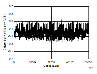
Histogram for Midscale Inputs (0V–6.144V) Figure 5-22 Typical DNL for All Codes
 Figure 5-24 Typical INL for All Codes (All Bipolar Ranges)
 Figure 5-26 INL
vs Temperature (All Bipolar Ranges)
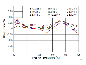
 Figure 5-28 Offset Error vs Temperature Across Input Ranges
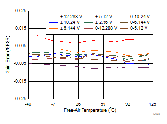
 Figure 5-30 Gain
Error vs Temperature Across Input Ranges
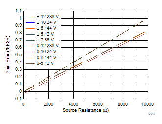
 Figure 5-32 Gain
Error vs External Resistance (REXT)
| Number of points = 500k, fIN = 1kHz |
Figure 5-34 Typical FFT Plot (All Ranges) for the ADS8685W Figure 5-36 SNR
vs Input Frequency
 Figure 5-38 THD
vs Input Frequency
 Figure 5-40 AVDD
Current vs Throughput
 Figure 5-42 AVDD
Current vs Temperature (Standby Mode)