SBASAY5 June   2024 ADS8681W

PRODUCTION DATA  

  1.   1
  2. Features
  3. Applications
  4. Description
  5. Pin Configuration and Functions
  6. Specifications
    1. 5.1 Absolute Maximum Ratings
    2. 5.2 ESD Ratings
    3. 5.3 Recommended Operating Conditions
    4. 5.4 Thermal Information
    5. 5.5 Electrical Characteristics
    6. 5.6 Timing Requirements
    7. 5.7 Timing Diagrams
    8. 5.8 Typical Characteristics
  7. Detailed Description
    1. 6.1 Overview
    2. 6.2 Functional Block Diagram
    3. 6.3 Feature Description
      1. 6.3.1 Analog Input Structure
      2. 6.3.2 Analog Input Impedance
      3. 6.3.3 Input Protection Circuit
      4. 6.3.4 Programmable Gain Amplifier (PGA)
      5. 6.3.5 Second-Order, Low-Pass Filter (LPF)
      6. 6.3.6 ADC Driver
      7. 6.3.7 Reference
        1. 6.3.7.1 Internal Reference
        2. 6.3.7.2 External Reference
      8. 6.3.8 ADC Transfer Function
      9. 6.3.9 Alarm Features
        1. 6.3.9.1 Input Alarm
        2. 6.3.9.2 AVDD Alarm
    4. 6.4 Device Functional Modes
      1. 6.4.1 Host-to-Device Connection Topologies
        1. 6.4.1.1 Single Device: All multiSPI Options
        2. 6.4.1.2 Single Device: Standard SPI Interface
        3. 6.4.1.3 Multiple Devices: Daisy-Chain Topology
      2. 6.4.2 Device Operational Modes
        1. 6.4.2.1 RESET State
        2. 6.4.2.2 ACQ State
        3. 6.4.2.3 CONV State
    5. 6.5 Programming
      1. 6.5.1 Data Transfer Frame
      2. 6.5.2 Input Command Word and Register Write Operation
      3. 6.5.3 Output Data Word
      4. 6.5.4 Data Transfer Protocols
        1. 6.5.4.1 Protocols for Configuring the Device
        2. 6.5.4.2 Protocols for Reading From the Device
          1. 6.5.4.2.1 Legacy, SPI-Compatible (SYS-xy-S) Protocols With a Single SDO-x
          2. 6.5.4.2.2 Legacy, SPI-Compatible (SYS-xy-S) Protocols With Dual SDO-x
          3. 6.5.4.2.3 Source-Synchronous (SRC) Protocols
            1. 6.5.4.2.3.1 Output Clock Source Options
            2. 6.5.4.2.3.2 Output Bus Width Options
  8. Register Maps
    1. 7.1 Device Configuration and Register Maps
      1. 7.1.1 DEVICE_ID_REG Register (address = 00h)
      2. 7.1.2 RST_PWRCTL_REG Register (address = 04h)
      3. 7.1.3 SDI_CTL_REG Register (address = 08h)
      4. 7.1.4 SDO_CTL_REG Register (address = 0Ch)
      5. 7.1.5 DATAOUT_CTL_REG Register (address = 10h)
      6. 7.1.6 RANGE_SEL_REG Register (address = 14h)
      7. 7.1.7 ALARM_REG Register (address = 20h)
      8. 7.1.8 ALARM_H_TH_REG Register (address = 24h)
      9. 7.1.9 ALARM_L_TH_REG Register (address = 28h)
  9. Application and Implementation
    1. 8.1 Application Information
    2. 8.2 Typical Application
      1. 8.2.1 Design Requirements
      2. 8.2.2 Detailed Design Procedure
        1. 8.2.2.1 Alarm Function
      3. 8.2.3 Application Curve
    3. 8.3 Power Supply Recommendations
      1. 8.3.1 Power Supply Decoupling
      2. 8.3.2 Power Saving
        1. 8.3.2.1 NAP Mode
        2. 8.3.2.2 Power-Down (PD) Mode
    4. 8.4 Layout
      1. 8.4.1 Layout Guidelines
      2. 8.4.2 Layout Example
  10. Device and Documentation Support
    1. 9.1 Documentation Support
      1. 9.1.1 Related Documentation
    2. 9.2 Receiving Notification of Documentation Updates
    3. 9.3 Support Resources
    4. 9.4 Trademarks
    5. 9.5 Electrostatic Discharge Caution
    6. 9.6 Glossary
  11. 10Revision History
  12. 11Mechanical, Packaging, and Orderable Information

Package Options

Mechanical Data (Package|Pins)
Thermal pad, mechanical data (Package|Pins)
Orderable Information
Legacy, SPI-Compatible (SYS-xy-S) Protocols With Dual SDO-x

Optionally, the device increases the SDO-x bus width from one bit to two bits (dual SDO-x) when operating with any data transfer protocol. The default bus width is one bit (single SDO-x). To operate the device in dual SDO mode, set the SDO1_CONFIG[1:0] bits in the SDO_CTL_REG register to 11b. In this mode, the ALARM/SDO-1/GPO pin functions as SDO-1.

In dual SDO mode, two bits of data are launched on the two SDO-x pins (SDO-0 and SDO-1) on every SCLK launch edge. Figure 6-16 and Figure 6-31 show timing diagrams for dual SDO mode.
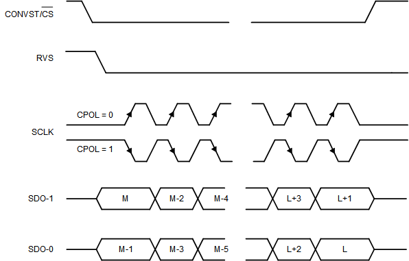
ADS8681W ADS8685W ADS8689W Standard SPI Timing Protocol(CPHA = 0, Dual
                        SDO-x)
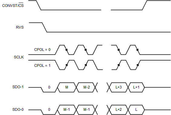
Figure 6-30 Standard SPI Timing Protocol
(CPHA = 0, Dual SDO-x)
ADS8681W ADS8685W ADS8689W Standard SPI Timing Protocol(CPHA = 1, Dual
                        SDO-x)Figure 6-31 Standard SPI Timing Protocol
(CPHA = 1, Dual SDO-x)
Note:

For any particular SPI protocol, the device follows the same timing specifications for single and dual SDO modes. The only difference is that the device requires half as many SCLK cycles to output the same number of bits when in single SDO mode. Thus, the minimum required SCLK frequency is reduced for a certain sampling rate of the ADC.