SBASAY5 June 2024 ADS8681W
PRODUCTION DATA
- 1
- 1 Features
- 2 Applications
- 3 Description
- 4 Pin Configuration and Functions
- 5 Specifications
-
6 Detailed Description
- 6.1 Overview
- 6.2 Functional Block Diagram
- 6.3 Feature Description
- 6.4 Device Functional Modes
- 6.5 Programming
-
7 Register Maps
- 7.1
Device Configuration and Register Maps
- 7.1.1 DEVICE_ID_REG Register (address = 00h)
- 7.1.2 RST_PWRCTL_REG Register (address = 04h)
- 7.1.3 SDI_CTL_REG Register (address = 08h)
- 7.1.4 SDO_CTL_REG Register (address = 0Ch)
- 7.1.5 DATAOUT_CTL_REG Register (address = 10h)
- 7.1.6 RANGE_SEL_REG Register (address = 14h)
- 7.1.7 ALARM_REG Register (address = 20h)
- 7.1.8 ALARM_H_TH_REG Register (address = 24h)
- 7.1.9 ALARM_L_TH_REG Register (address = 28h)
- 7.1
Device Configuration and Register Maps
- 8 Application and Implementation
- 9 Device and Documentation Support
- 10Revision History
- 11Mechanical, Packaging, and Orderable Information
Package Options
Mechanical Data (Package|Pins)
- RUM|16
Thermal pad, mechanical data (Package|Pins)
- RUM|16
Orderable Information
6.3.9 Alarm Features
The device features an active-high alarm output on the ALARM/SDO-1/GPO pin, provided that the pin is configured for alarm functionality. To enable the ALARM output on the multifunction pin, set the SDO1_CONFIG[1:0] bits of the SDO_CTL_REG register to 01b.
The device features two types of alarm functions: an input alarm and an AVDD alarm.
- For the input alarm, the voltage at the ADC input is monitored and compared against user-programmable high and low threshold values. The device sets an active high alarm output when the corresponding digital value of the input signal goes beyond the high or low threshold set by the user. See the Input Alarm section for a detailed explanation of the input alarm feature functionality.
- For the AVDD alarm, the ADC analog supply voltage (AVDD) is monitored and compared against the specified typical threshold values of the AVDD supply. The low threshold value is 4.7V and the high threshold value is 5.3V. The device sets an active high alarm output if the AVDD value crosses the specified low (4.7V) or high threshold (5.3V) values in either direction.
When the alarm functionality is turned on, both the input and AVDD alarm functions are enabled by default. These alarm functions are selectively disabled by programming the IN_AL_DIS and VDD_AL_DIS bits (respectively) of the RST_PWRCTL_REG register.
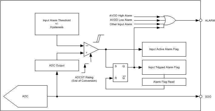
Each alarm (input or AVDD) has two associated types of alarm flags: the active alarm flag and the tripped alarm flag. All alarm flags are read in the ALARM_REG register. Both flags are set when the associated alarm is triggered. The active alarm is cleared at the end of the current ADC conversion (and set again if the alarm condition persists). However, the tripped flag is cleared only after ALARM_REG is read.
The ALARM output flags are updated internally at the end of every conversion. These output flags are read during any data frame that the user initiates by bringing the CONVST/CS signal to a low level.
Read the ALARM output flags in three different ways. Read these flags with the ALARM output pin, by reading the internal ALARM registers, or by appending the ALARM flags to the data output.
- A high level on the ALARM pin indicates an over- or undervoltage condition on AVDD or on the analog input channel of the device. This pin is able to be wired to interrupt the host input.
- The internal ALARM flag bits in the ALARM_REG register are updated at the end of conversion. After receiving an ALARM interrupt on the output pin, read the internal alarm flag registers for more details on the conditions that generated the alarm.
- The alarm output flags are selectively appended to the data output bit stream (see the DATAOUT_CTL_REG register for configuration details).
Figure 6-16 depicts a functional block diagram for the device alarm functionality.
 Figure 6-16 Alarm Functionality Schematic