SBASAY5 June 2024 ADS8681W
PRODUCTION DATA
- 1
- 1 Features
- 2 Applications
- 3 Description
- 4 Pin Configuration and Functions
- 5 Specifications
-
6 Detailed Description
- 6.1 Overview
- 6.2 Functional Block Diagram
- 6.3 Feature Description
- 6.4 Device Functional Modes
- 6.5 Programming
-
7 Register Maps
- 7.1
Device Configuration and Register Maps
- 7.1.1 DEVICE_ID_REG Register (address = 00h)
- 7.1.2 RST_PWRCTL_REG Register (address = 04h)
- 7.1.3 SDI_CTL_REG Register (address = 08h)
- 7.1.4 SDO_CTL_REG Register (address = 0Ch)
- 7.1.5 DATAOUT_CTL_REG Register (address = 10h)
- 7.1.6 RANGE_SEL_REG Register (address = 14h)
- 7.1.7 ALARM_REG Register (address = 20h)
- 7.1.8 ALARM_H_TH_REG Register (address = 24h)
- 7.1.9 ALARM_L_TH_REG Register (address = 28h)
- 7.1
Device Configuration and Register Maps
- 8 Application and Implementation
- 9 Device and Documentation Support
- 10Revision History
- 11Mechanical, Packaging, and Orderable Information
Package Options
Mechanical Data (Package|Pins)
- RUM|16
Thermal pad, mechanical data (Package|Pins)
- RUM|16
Orderable Information
6.3.7.2 External Reference
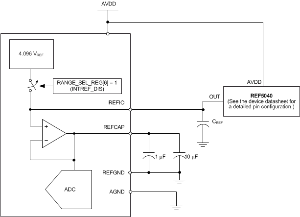
The device provides a provision for applications that require a better reference voltage or a common reference voltage for multiple devices. This provision allows an external reference source to be used with an internal buffer to drive the ADC reference pin. To select the external reference mode, program the INTREF_DIS bit of the RANGE_SEL_REG register to logic 1. In this mode, apply an external 4.096V reference at the REFIO pin, which functions as an input. The internal buffer is optimally designed to handle the dynamic loading on the REFCAP pin that is internally connected to the ADC reference input. Thus, any low-power, low-drift, or small-size external reference is applicable in this mode. Appropriately filter the output of the external reference to minimize the resulting effect of the reference noise on system performance. Figure 6-12 shows a typical connection diagram for this mode.
 Figure 6-12 Device Connections for
Using an External 4.096V Reference
Figure 6-12 Device Connections for
Using an External 4.096V ReferenceThe output of the internal reference buffer appears at the REFCAP pin. Place a 10µF minimum capacitance between the REFCAP and REFGND pins. Place another 1µF capacitor as close to the REFCAP pin as possible for decoupling high-frequency signals. Do not use the internal buffer to drive external ac or dc loads because of the limited current output capability of this buffer.
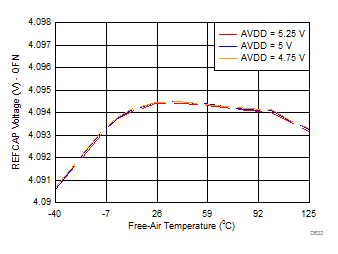
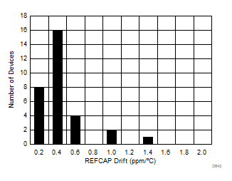
The performance of the internal buffer output is very stable across the entire operating temperature range of –40°C to +125°C. Figure 6-13 shows the variation in the REFCAP output across temperature for different values of the AVDD supply voltage. As shown in Figure 6-14, the typical specified value of the reference buffer drift over temperature is 0.5ppm/°C. The maximum specified temperature drift is equal to 2ppm/°C.


| AVDD = 5V, number of devices = 30, ΔT = –40°C to +125°C |