SBASAY5 June 2024 ADS8681W
PRODUCTION DATA
- 1
- 1 Features
- 2 Applications
- 3 Description
- 4 Pin Configuration and Functions
- 5 Specifications
-
6 Detailed Description
- 6.1 Overview
- 6.2 Functional Block Diagram
- 6.3 Feature Description
- 6.4 Device Functional Modes
- 6.5 Programming
-
7 Register Maps
- 7.1
Device Configuration and Register Maps
- 7.1.1 DEVICE_ID_REG Register (address = 00h)
- 7.1.2 RST_PWRCTL_REG Register (address = 04h)
- 7.1.3 SDI_CTL_REG Register (address = 08h)
- 7.1.4 SDO_CTL_REG Register (address = 0Ch)
- 7.1.5 DATAOUT_CTL_REG Register (address = 10h)
- 7.1.6 RANGE_SEL_REG Register (address = 14h)
- 7.1.7 ALARM_REG Register (address = 20h)
- 7.1.8 ALARM_H_TH_REG Register (address = 24h)
- 7.1.9 ALARM_L_TH_REG Register (address = 28h)
- 7.1
Device Configuration and Register Maps
- 8 Application and Implementation
- 9 Device and Documentation Support
- 10Revision History
- 11Mechanical, Packaging, and Orderable Information
Package Options
Mechanical Data (Package|Pins)
- RUM|16
Thermal pad, mechanical data (Package|Pins)
- RUM|16
Orderable Information
6.3.7.1 Internal Reference
The device features an internal reference source with a nominal output value of 4.096V. To select the internal reference, program the INTREF_DIS bit of the RANGE_SEL_REG register to logic 0. When the internal reference is used, the REFIO pin becomes an output with the internal reference value. As shown in Figure 6-7, place a 4.7µF (minimum) decoupling capacitor between the REFIO and REFGND pins. The output impedance of the internal band-gap circuit creates a low-pass filter with this capacitor to band-limit the noise of the reference. Using a smaller capacitor value allows higher reference noise in the system that potentially degrades SNR and SINAD performance. Do not use the REFIO pin to drive external ac or dc loads because of limited current output capability. Use the REFIO pin as a source if followed by an acceptable op amp buffer (such as the OPA320).
 Figure 6-7 Device
Connections for Using an Internal 4.096V Reference
Figure 6-7 Device
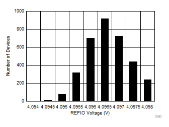
Connections for Using an Internal 4.096V ReferenceThe device internal reference is factory-trimmed to provide the initial accuracy specification. The histogram in Figure 6-8 shows the distribution of the internal voltage reference output taken from more than 3420 production devices.

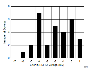
The initial accuracy specification for the internal reference is degraded if the die is exposed to any mechanical or thermal stress. Heating the device while soldering to a printed circuit board (PCB) and any subsequent solder reflow is a primary cause for shifts in the VREF value. The main cause of thermal hysteresis is a change in die stress and is a function of the package, die-attach material, molding compound, and device layout.
To illustrate this effect, 30 devices were soldered using lead-free solder paste with the manufacturer suggested reflow profile. This process is explained in the AN-2029 Handling and Process Recommendations application note. As shown in Figure 6-9, the internal voltage reference output is measured before and after the reflow process and the typical shift in value. Although all tested units exhibit a positive shift in the output voltages, negative shifts are also possible. The histogram in Figure 6-9 shows the typical shift for exposure to a single reflow profile. Exposure to multiple reflows, which is common on PCBs with surface-mount components on both sides, causes additional shifts in the output voltage. If the PCB is to be exposed to multiple reflows, solder the ADS868xW in the second pass to minimize device exposure to thermal stress.

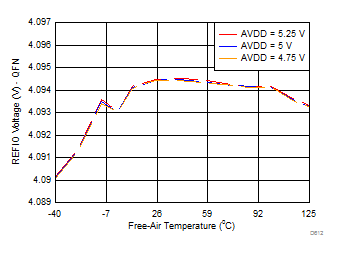
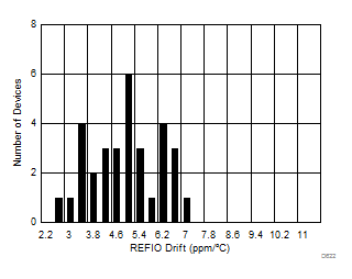
The internal reference is also temperature compensated to provide excellent temperature drift over an extended industrial temperature range of –40°C to +125°C. Figure 6-10 shows the variation of the internal reference voltage across temperature for different values of the AVDD supply voltage. Figure 6-11 shows histogram distribution of the reference voltage drift for the WQFN (RUM) package.


| AVDD = 5V, number of devices = 30, ΔT = –40°C to +125°C |