SBAS633E February 2016 – August 2022 ADS8681 , ADS8685 , ADS8689
PRODUCTION DATA
- 1 Features
- 2 Applications
- 3 Description
- 4 Revision History
- 5 Pin Configuration and Functions
-
6 Specifications
- 6.1 Absolute Maximum Ratings
- 6.2 ESD Ratings
- 6.3 Recommended Operating Conditions
- 6.4 Thermal Information
- 6.5 Electrical Characteristics
- 6.6 Timing Requirements: Conversion Cycle
- 6.7 Timing Requirements: Asynchronous Reset
- 6.8 Timing Requirements: SPI-Compatible Serial Interface
- 6.9 Timing Requirements: Source-Synchronous Serial Interface (External Clock)
- 6.10 Timing Requirements: Source-Synchronous Serial Interface (Internal Clock)
- 6.11 Timing Diagrams
- 6.12 Typical Characteristics
-
7 Detailed Description
- 7.1 Overview
- 7.2 Functional Block Diagram
- 7.3 Feature Description
- 7.4 Device Functional Modes
- 7.5 Programming
- 7.6
Register Maps
- 7.6.1
Device Configuration and Register Maps
- 7.6.1.1 DEVICE_ID_REG Register (address = 00h)
- 7.6.1.2 RST_PWRCTL_REG Register (address = 04h)
- 7.6.1.3 SDI_CTL_REG Register (address = 08h)
- 7.6.1.4 SDO_CTL_REG Register (address = 0Ch)
- 7.6.1.5 DATAOUT_CTL_REG Register (address = 10h)
- 7.6.1.6 RANGE_SEL_REG Register (address = 14h)
- 7.6.1.7 ALARM_REG Register (address = 20h)
- 7.6.1.8 ALARM_H_TH_REG Register (address = 24h)
- 7.6.1.9 ALARM_L_TH_REG Register (address = 28h)
- 7.6.1
Device Configuration and Register Maps
- 8 Application and Implementation
- 9 Device and Documentation Support
- 10Mechanical, Packaging, and Orderable Information
Package Options
Refer to the PDF data sheet for device specific package drawings
Mechanical Data (Package|Pins)
- PW|16
Thermal pad, mechanical data (Package|Pins)
Orderable Information
7.4 Device Functional Modes
The device features the multiSPI digital interface for communication and data transfer between the device and the host controller. The multiSPI interface supports many data transfer protocols that the host uses to exchange data and commands with the device. The host can transfer data into the device using one of the standard SPI modes. However, the device can be configured to output data in a number of ways to suit the application demands of throughput and latency. The data output in these modes can be controlled either by the host or the device, and the timing can either be system synchronous or source synchronous. For detailed explanation of the supported data transfer protocols, see the Section 7.5.4 section.
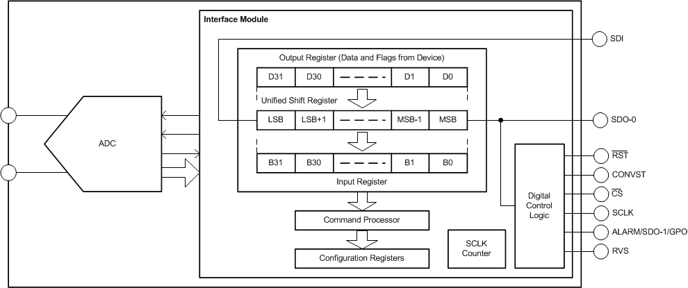
This section describes the main components of the digital interface module as well as supported configurations and protocols. As shown in Figure 7-23, the interface module is comprised of shift registers (both input and output), configuration registers, and a protocol unit. During any particular data frame, data are transferred both into and out of the device. As a result, the host always perceives the device as a 32-bit input-output shift register, as shown in Figure 7-23.
 Figure 7-23 Device Interface Module
The Section 5 section provides descriptions of the interface pins; the Section 7.5.1 section details the functions of shift registers, the SCLK counter, and the command processor; the Section 7.5.1 section details supported protocols; and the Section 7.6 section explains the configuration registers and bit settings.