SBAS614C May 2013 – March 2019 ADS8866
PRODUCTION DATA.
- 1 Features
- 2 Applications
- 3 Description
- 4 Revision History
- 5 Device Comparison Table
- 6 Pin Configuration and Functions
- 7 Specifications
- 8 Parameter Measurement Information
- 9 Detailed Description
- 10Application and Implementation
- 11Power Supply Recommendations
- 12Layout
- 13Device and Documentation Support
- 14Mechanical, Packaging, and Orderable Information
Package Options
Mechanical Data (Package|Pins)
Thermal pad, mechanical data (Package|Pins)
- DRC|10
Orderable Information
9.4.2.1 Daisy-Chain Mode
This interface option is most useful in applications where multiple ADC devices are used but the digital host has limited interfacing capability. Figure 49 shows a connection diagram with N ADCs connected in the daisy-chain. The CONVST pins of all ADCs in the chain are connected together and are controlled by a single pin of the digital host. Similarly, the SCLK pins of all ADCs in the chain are connected together and are controlled by a single pin of the digital host. The DIN pin for ADC 1 (DIN-1) is connected to GND. The DOUT pin of ADC 1 (DOUT-1) is connected to the DIN pin of ADC 2 (DIN-2), and so on. The DOUT pin of the last ADC in the chain (DOUT-N) is connected to the SDI pin of the digital host.
 Figure 49. Connection Diagram: Daisy-Chain Mode (DIN = 0)
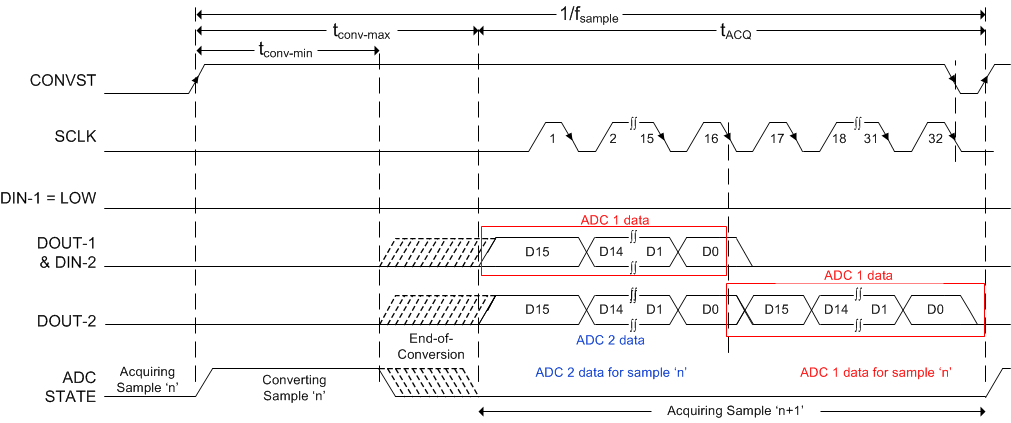
 As shown in Figure 50, the device DOUT pin is driven low when DIN and CONVST are low together. With DIN low, a CONVST rising edge selects daisy-chain mode, samples the analog input, and causes the device to enter a conversion phase. In this interface option, CONVST must remain high from the start of the conversion until all data bits are read. When started, the conversion continues regardless of the state of SCLK, however SCLK must be low at the CONVST rising edge.
 Figure 50. Interface Timing Diagram: For Two Devices in Daisy-Chain Mode
 At the end of conversion, every ADC in the chain loads its own conversion result into the internal, 16-bit, shift register and also outputs the MSB bit of this conversion result on its own DOUT pin. All ADCs enter an acquisition phase and power-down. On every subsequent SCLK falling edge, the internal shift register of each ADC latches the data available on its DIN pin and shifts out the next bit of data on its DOUT pin. Therefore, the digital host receives the data of ADC N, followed by the data of ADC N–1, and so on (in MSB-first fashion). A total of 16 x N SCLK falling edges are required to capture the outputs of all N devices in the chain. Data can be read at either SCLK falling or rising edges. Note that with any SCLK frequency, reading data at SCLK falling edge requires the digital host to clock in the data during the th_CK_DO-min time frame.